Bootstrap circuit, and shift register, scanning circuit, display device using the same

a technology of shift register and display device, which is applied in the field of bootstrap circuit, can solve the problems of increasing power consumption of charging and discharging holding capacitors, requiring a large number of steps in the process, and reducing so as to reduce the power consumption of devices and reduce the power consumption. , the effect of large capacity

Active Publication Date: 2006-11-23
NEC LCD TECH CORP
View PDF7 Cites 58 Cited by
  • Summary
  • Abstract
  • Description
  • Claims
  • Application Information

AI Technical Summary

Benefits of technology

[0071] With the present invention, it is not necessary for the gate electrode of the output transistor to have the holding capacitor with a large capacity, and there is no electric current frown from the positive power source (high level) side to the negative power source (low level) side through the transistor. Therefore, the power consumption can be reduced. As a result, when applying the shift register of the present invention to a display device, power consumption of the device can be reduced.
[0072] The second effect is that the circuit can be downsized since the holding capacitor of a large capacity can be eliminated. As a result, a display device with a screen of high resolution can be achieved by applying the shift register of the present invention to the display device.
[0073] The third effect is that the reliability of the transistor can be improved since the voltage applied between the source and drain, between the gate and source, and between the gate and drain of the transistors can be decreased. As a result, when it is applied to the display device or the like, the reliability of the device can be improved.
[0074] The fourth effect is that it is possible to suppress the deterioration in the output amplitude even if there is a fluctuation in the transistor characteristic. Thus, when used for constituting a scanning circuit, it is possible to suppress such an operation failure that the amplitude is deteriorated for every single stage and that it becomes impossible to carry out the shift action at last. Furthermore, when applied to the display device or the like, it allows suppression of operation failure. Therefore, the reliability of the device can be improved.

Problems solved by technology

However, there is such a shortcoming in the manufacture process of the CMOS that there requires a great number of steps in the process for fabricating both the N-channel type transistors and the P-channel type transistors.
The circuit area becomes large as a result and it is difficult to downsize the circuit.
Further, the power consumption is increased for charging and discharging the holding capacitor C101 that has the large capacity.
However, an electric current is flown from the positive power source (DD terminal) to the negative power source (SS terminal) through the transistors 26 and 23, thereby increasing the power consumption like the above-described conventional case.
Furthermore, since the output is used as the input of the next stage in the conventional shift register, the voltage amplitude of the output signal is deteriorated when the transistor characteristic fluctuates (the driving capacity is decreased).

Method used


Image

  • Bootstrap circuit, and shift register, scanning circuit, display device using the same
  • Bootstrap circuit, and shift register, scanning circuit, display device using the same
  • Bootstrap circuit, and shift register, scanning circuit, display device using the same

Examples


first embodiment

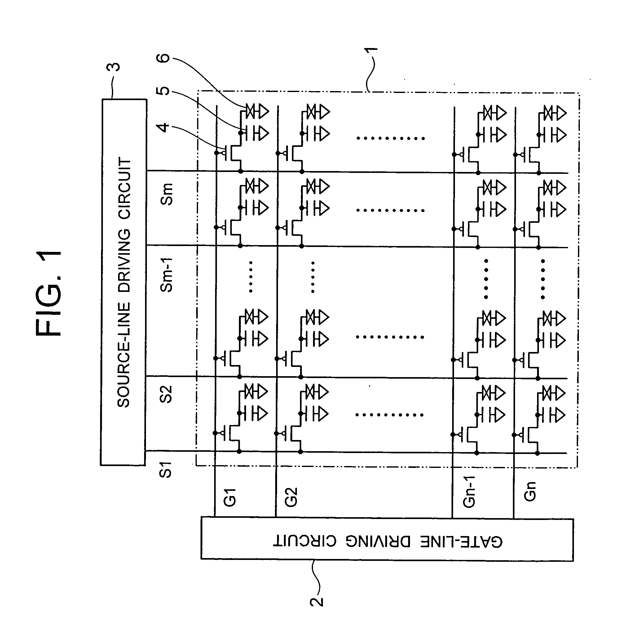
[0110] As shown in FIG. 1, a liquid crystal display device to which the embodiment of the present invention is applied comprises a pixel unit 1, a gate-line driving circuit 2, and a source-line driving circuit 3. The pixel unit 1, the gate-line driving circuit 2 and the source-line driving circuit 3 are formed on a same glass substrate.

[0111] The pixel unit 1 has gate lines G1-Gn and source lines S1-Sm being orthogonal to each other formed thereon. Terminals of the gate-line driving circuit 2 are connected to the corresponding gate lines G1-Gn. Further, terminals of the source-line driving circuit 3 are connected to the corresponding source lines S1-Sm. Furthermore, at each node between the gate lines G1-Gn and the source lines S1-Sm within the pixel unit 1, there is disposed a pixel circuit which is constituted with a pixel transistor 4 (a polysilicon transistor), a pixel accumulating capacity 5, and a pixel capacity 6 made of liquid crystal.

[0112] The gate-line driving circuit 2...

second embodiment

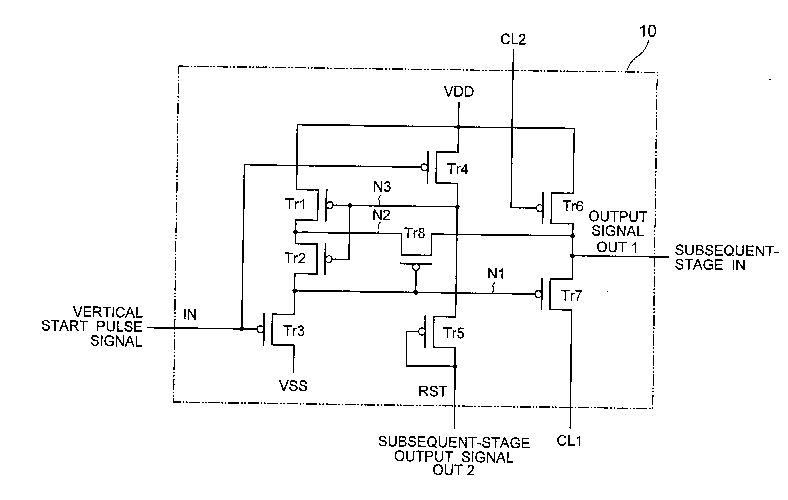
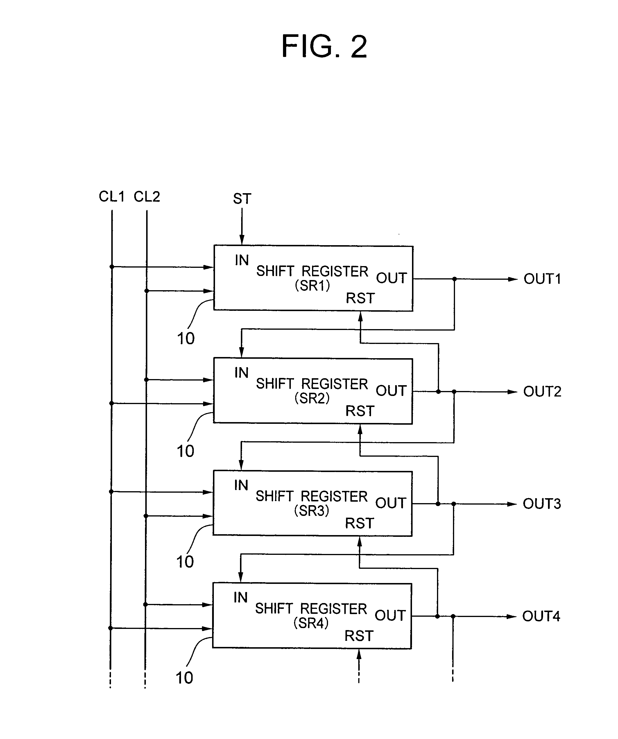
[0134]FIG. 5 shows the configuration of the scanning circuit according to a second embodiment of the present invention, and FIG. 6 shows the configuration of the shift register that constitutes the scanning circuit.

[0135] As shown in FIG. 5, the scanning circuit according to the second embodiment of the present invention is constituted with a plurality of shift registers 11 connected in series. As shown in FIG. 6, the shift register 11 has transistors Tr9 and Tr10 added to the subsequent-stages of the transistors Tr6 and Tr7 in the circuit of the shift register 10 shown in FIG. 3. The second embodiment of the present invention is distinctive in respect that there is outputted a transfer output signal OUT B as a transfer output for the next stage at a timing of outputting an output signal OUT A (scanning output signal OUT A) by adding the transistors Tr9 and Tr10. FIG. 6 illustrates the configuration of the first-stage shift register 11, however, the configuration of circuits of the...

third embodiment

[0140]FIG. 7 shows the configuration of the shift register according to a third embodiment of the present invention. The configuration of the scanning circuit constituted by combining a plurality of the shift registers shown in FIG. 7 is the same as the one shown in FIG. 2, and the timing chart thereof is the same as the one shown in FIG. 4.

[0141] In the shift register of FIG. 7 according to the third embodiment of the present invention, the transistor Tr8 is eliminated from the circuit structure of the shift register of FIG. 3 according to the first embodiment, and the node N2 is directly connected to the output terminal from which the output signal OUT is outputted.

[0142] Therefore, the third embodiment of the present invention is advantageous compared to the shift register of the first embodiment shown in FIG. 2 in respect that it allows the total number of the transistors to be reduced, thereby enabling the circuit to be downsized. The shift register according to the third emb...


PUM


Abstract

There is disclosed a shift register comprising a bootstrap circuit that outputs a voltage of the supply voltage to the output when the voltage of a first node becomes higher or lower than the supply voltage. The shift register comprises: two or more transistors connected in series to the first node; a device for supplying the voltage to a second node between the transistors such that the voltage between the drains and sources of the transistors becomes below the supply voltage; a first input transistor connected to the first node, and the gate electrode thereof is connected to a first input terminal as well; and an output transistor connected to the output terminal and the clock signal while having the gate electrode connected to the first node, wherein the gate electrode of the output transistor is not opened except for the bootstrap period.

Description

BACKGROUND OF THE INVENTION [0001] 1. Field of the Invention [0002] The present invention relates to a bootstrap circuit and the like, which are preferable for a driving circuit of a display device such as a liquid crystal display device, an organic EL display device, etc. [0003] 2. Description of the Related Art [0004] Recently, there has been a wide spread of an active-matrix type display device having thin-film transistors as active elements integrated on each pixel. Particularly, an active-type liquid crystal device using polysilicon transistors has become popular for portable devices such as a portable telephone and the like, since it allows size reduction of the device. The polysilicon thin-film transistor exhibits higher mobility than that of an amorphous silicon thin-film transistor. Therefore, not only pixel transistors for constituting the pixels but also the driving circuit can be formed easily in the periphery of the pixel unit by the same manufacture process. As the dri...

Claims


Application Information

Patent Timeline
Patent Type & Authority Applications(United States)
IPC IPC(8): G09G3/36
CPCG11C19/28
Inventor SHIMODA, MASAMICHI
Owner NEC LCD TECH CORP
Why Eureka
Try Eureka