Method of designing semiconductor device, semiconductor device and recording medium

a semiconductor and recording medium technology, applied in the field of semiconductor devices, can solve the problems of stringent requirements, electric isolation between the element regions, affecting the operating speed of such mos transistors, etc., and achieve the effect of high impurity concentration

Inactive Publication Date: 2006-11-30
RENESAS TECH CORP
View PDF9 Cites 7 Cited by
  • Summary
  • Abstract
  • Description
  • Claims
  • Application Information

AI Technical Summary

Benefits of technology

[0036] As described hereinabove, in the method of the first aspect of the present invention, the layout pattern of the MOS transistor is determined in the step (b) so as to satisfy the conditional expression R·C·f<1 where C=the gate capacitance (F) of the MOS transistor, R=the resistance (Ωm) of the fixed potential transmission path extending from the at least one body contact to the body region, f=the operating frequency (Hz) of the predetermined clock, and f≧500 MHz. This allows the design of the body potential fixed MOS transistor which is stable in operating speed also during the high-speed operation thereof.
[0063] The recording medium in accordance with the seventeenth aspect of the present invention records thereon the program for embodying the method of the first or second aspects. Thus, the execution of the program by a computer allows the design of a body potential fixed MOS transistor or MOS transistor having the short-circuited gate electrode and body portion which is stable in operating speed also during the high-speed operation thereof.

Problems solved by technology

This results in electrical isolation between the element regions.
However, a high-speed operation in synchronism with a clock having an operating frequency of not less than 500 MHz imposes very stringent requirements for the timing of signal passing between circuits.
This phenomenon affects the operating speed of such MOS transistors, for example, an unstable operation thereof.

Method used


Image

  • Method of designing semiconductor device, semiconductor device and recording medium
  • Method of designing semiconductor device, semiconductor device and recording medium
  • Method of designing semiconductor device, semiconductor device and recording medium

Examples


first preferred embodiment

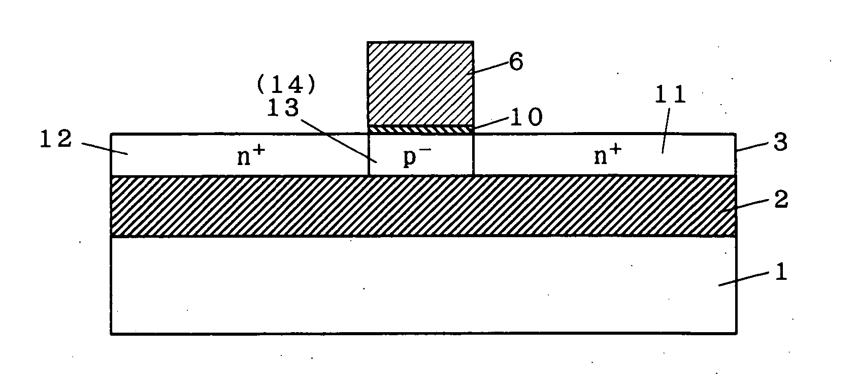
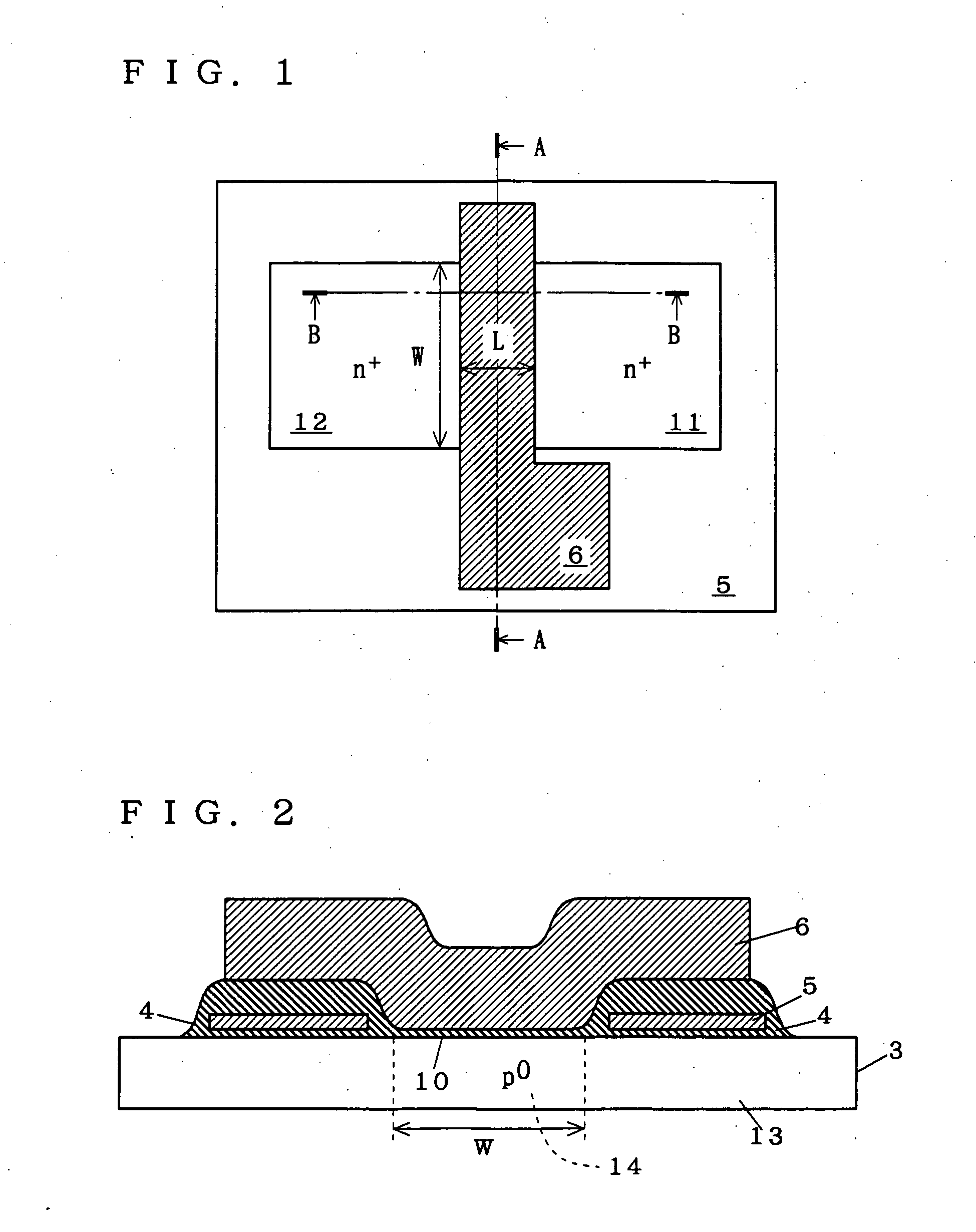
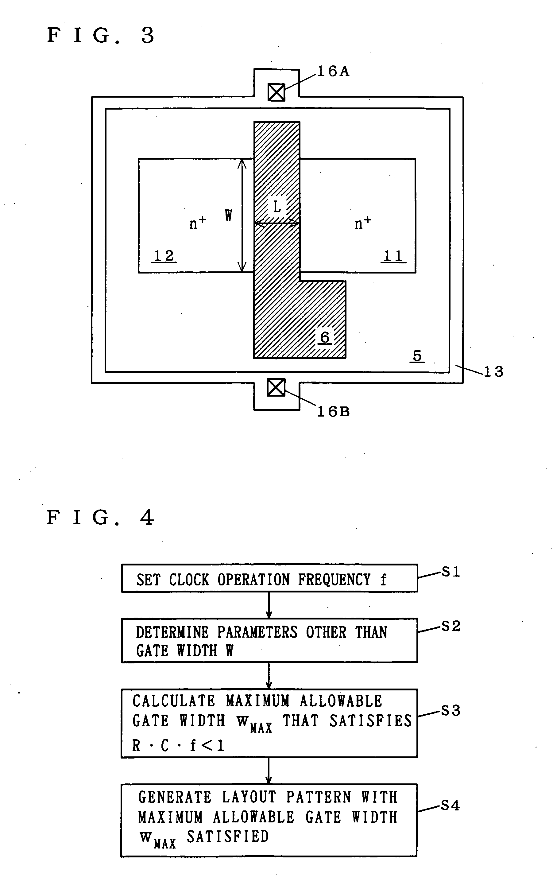
[0090]FIG. 1 is a plan view of an NMOS transistor having an SOI structure employing FS isolation which is designed by a semiconductor device designing method according to a first preferred embodiment of the present invention. FIG. 2 is a cross-sectional view taken along the line A-A of FIG. 1. As shown in FIGS. 1 and 2, an FS electrode 5 is formed on an FS insulating layer 4 provided on part of a body portion 13 which lies on the periphery of and adjacent to an N-type drain region 11 and an N-type source region 12. The body portion 13 is defined to include a body region 14 between the drain region 11 and the source region 12, and a P-type region extending from the body region 14.

[0091] A gate electrode 6 is formed over the body region 14 and parts of the FS electrode 5. The gate electrode 6 is formed over the body region 14 with a gate oxide film 10 therebetween, and is formed over the parts of the FS electrode 5 with the FS insulating layer 4 therebetween. Although not shown in FI...

second preferred embodiment

[0118] The result of simulation, similar to that of the first preferred embodiment, which is based on a signal propagation delay time tpd (s) required for a single DT MOS transistor having the gate capacitance C (F) and body resistance R (Ω) determined in Expressions (1) and (2) has revealed that the DT MOS transistor operates in a stable state also during the high-speed operation with the signal propagation delay time tpd of not greater than 50 ps if conditions represented by Expression (6) are satisfied. R·Ctpd<1(6)

[0119] For instance, if ρ=0.08 (Ω·cm), K0=3.9, ε0=8.86×10⁻⁴ (F / cm), and tpd=50 (ps), then the gate width W, the gate oxide film thickness tOX, and the SOI layer thickness tSOI should satisfy conditions expressed by W2tOX·tSOI<tpdρ·K0·ɛ0=1.8⨯103(7)

[0120] Then, if the gate oxide film thickness tOX=0.007 (μm) and the SOI layer thickness tSOI=0.1 (μm), the restrictive condition (iii) that {W2<1.26}, or {W<1.12 (μm)}, should be satisfied.

[0121] When a short circuit ...

third preferred embodiment

[0134] The first and second preferred embodiments illustrate the restrictive conditions of the gate width W, gate oxide film thickness tOX and SOI layer thickness tSOI of the (DT) MOS transistor having the SOI structure which achieves the stable operation by fixing the body potential. Third to tenth preferred embodiments to be described below are intended for improvements in other parameters in Expression (3) or (6) and addition of structural ingenuity for setting of a greater gate width W.

[0135]FIGS. 8 and 9 are cross-sectional views of the MOS transistor having the SOI structure according to the third preferred embodiment of the present invention. The cross section of FIG. 8 corresponds to that taken along the line A-A of FIG. 1, and the cross section of FIG. 9 corresponds to that taken along the line B-B of FIG. 1.

[0136] Referring to FIG. 9, the drain region 11 and the source region 12 are selectively formed so as to extend vertically through the SOI layer 3. The gate oxide fil...


PUM


Abstract

A semiconductor device including a transistor having an SOI structure the operating speed of which is not affected is provided. A MOS transistor having the SOI structure is formed which satisfies R·C·f<1 where C is a gate capacitance (F), R is a body resistance (Ω), f is a clock operating frequency (Hz), and f≧500 MHz.

Description

BACKGROUND OF THE INVENTION [0001] 1. Field of the Invention [0002] The present invention relates to a semiconductor device having a MOS transistor formed on an SOI substrate. [0003] 2. Description of the Background Art [0004]FIG. 20 is a perspective view showing a cross section of a conventional semiconductor device M90 having a field isolation structure which is the background of the present invention. The semiconductor device M90 is an SOI semiconductor device in which an SOI substrate including a semiconductor layer in film form, or an SOI (semiconductor-on-insulator) layer, which is formed on an insulating substrate is used as a semiconductor substrate into which transistor elements and the like are manufactured. [0005] As shown in FIG. 20, the semiconductor device M90 comprises a silicon semiconductor layer as the SOI layer 3 formed on the insulating substrate including a supporting substrate 1 and a buried oxide film 2. The SOI layer 3 includes a great number of element regio...

Claims


Application Information

Patent Timeline
Patent Type & Authority Applications(United States)
IPC IPC(8): H01L27/12G06F17/50H01L21/762H01L21/336H01L21/765H01L27/02H01L29/423H01L29/786
CPCG06F17/5068H01L21/765H01L27/0207H01L27/1203H01L29/78654H01L29/42384H01L29/66772H01L29/78615H01L29/42372G06F30/39H01L21/18
Inventor MAEDA, SHIGENOBUYAMAGUCHI, YASUO
Owner RENESAS TECH CORP
Why Eureka
Try Eureka