Electro-optical device, method of manufacturing the same, and electronic apparatus

a technology of optical devices and electronic devices, applied in the direction of resistor housings/enclosements/embeddings, non-linear optics, instruments, etc., can solve the problem that the resistance value of the resistor pattern can be minutely adjusted in the liquid crystal display device, and achieve the effect of easy manufacturing of terminating resistors and high-accuracy terminating resistors

Inactive Publication Date: 2006-11-30
JAPAN DISPLAY WEST
View PDF14 Cites 8 Cited by
  • Summary
  • Abstract
  • Description
  • Claims
  • Application Information

AI Technical Summary

Benefits of technology

[0050] Therefore, it is possible to easily manufacture a terminating resistor by cutting at least one of the plurality of resistors, when the IC cannot receive suitable differential signals from an FPC through the pair of wiring lines according to the differential transmission scheme due to small resistance values of t

Problems solved by technology

Therefore, the liquid crystal display device has a limit in which i

Method used


Image

  • Electro-optical device, method of manufacturing the same, and electronic apparatus
  • Electro-optical device, method of manufacturing the same, and electronic apparatus
  • Electro-optical device, method of manufacturing the same, and electronic apparatus

Examples


first embodiment

Structure of Liquid Crystal Display Device

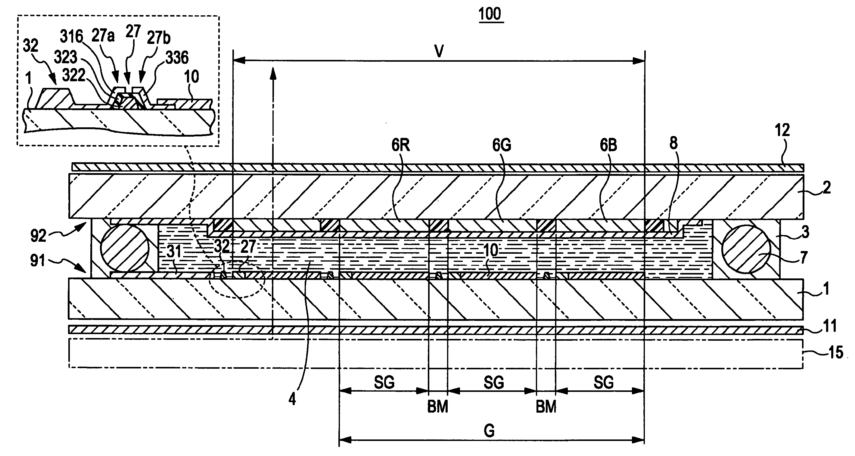
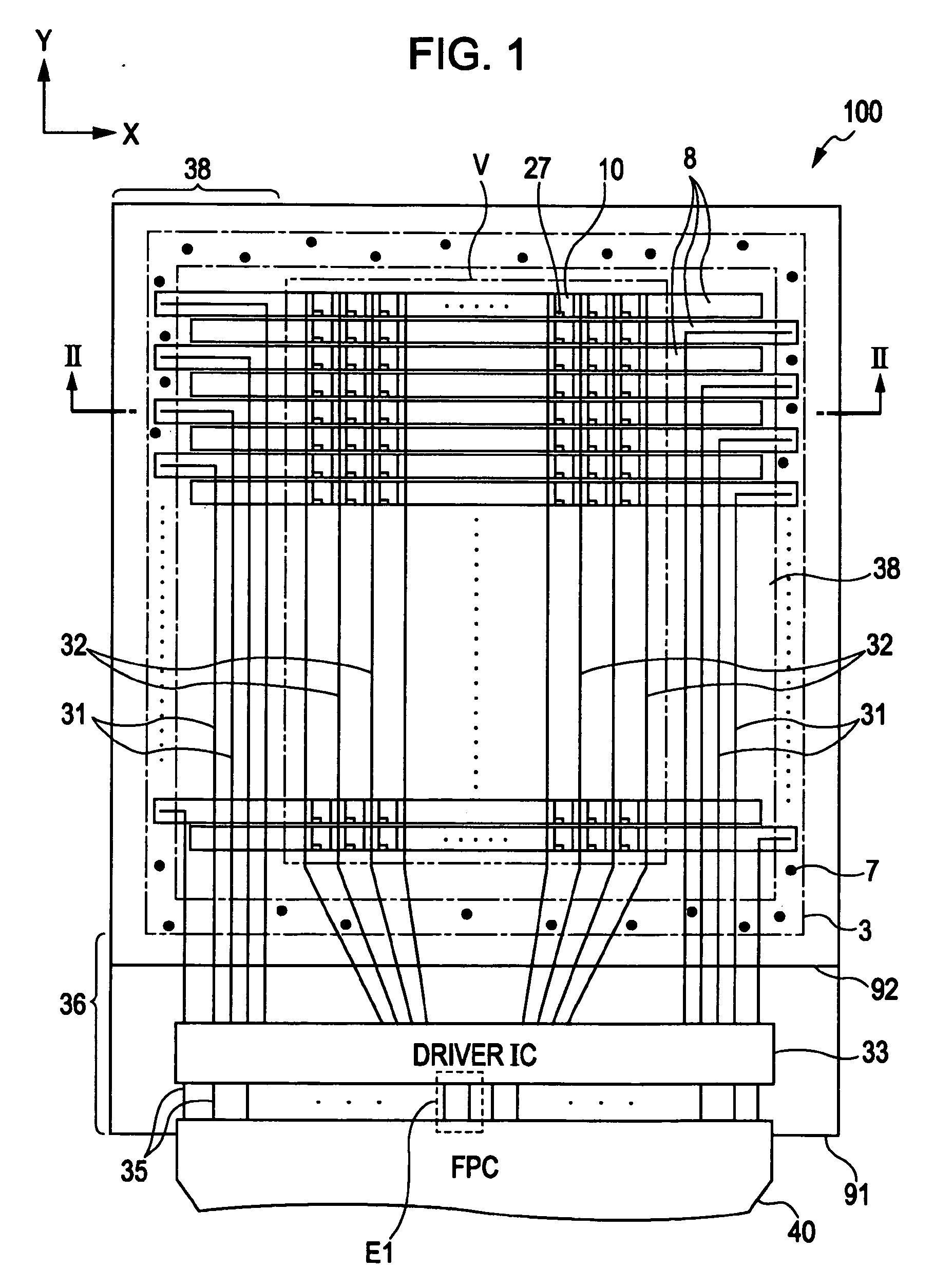
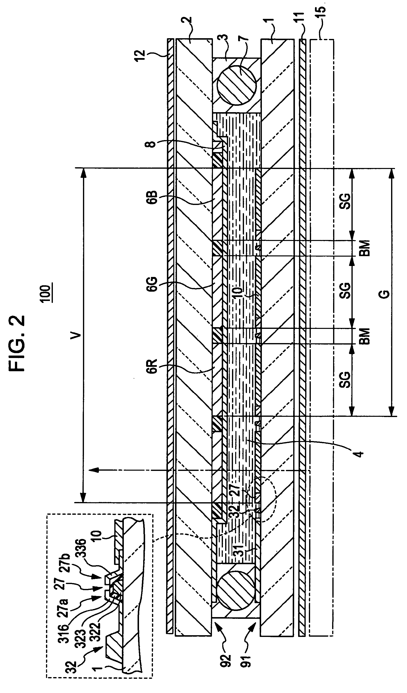
[0078] First, the structure of a liquid crystal display device according to a first embodiment of the invention will be described below. FIG. 1 is a plan view schematically illustrating the structure of a liquid crystal display device 100 according to the first embodiment of the invention. FIG. 1 mainly shows the structure of electrodes and wiring lines of the liquid crystal display device 100 in plan view. The liquid crystal display device 100 of the first embodiment is an active matrix driving type using thin film diodes (TFDs) and a transmissive type. FIG. 2 is a schematic cross-sectional view of the liquid crystal display device 100, taken along the line II-II of FIG. 1.

[0079] First, the sectional-view structure of the liquid crystal display device 100 will be described with reference to FIG. 2, and then the structure of the electrodes and the wiring lines of the liquid crystal display device 100 will be described.

[0080] In FIG. 2, t...

second embodiment

[0139] Next, a method of manufacturing a high-accuracy terminating resistor according to a second embodiment of the invention will be described below with reference to FIGS. 7A to 9G. More specifically, a description will be made below of a method of providing a wiring pattern whose length can freely vary by trimming at a position where a terminating resistor will be formed, and of trimming the wiring pattern to manufacture a terminating resistor. The second embodiment differs from the first embodiment in the structure of a pair of external connection wiring lines 35a and 35b. Therefore, in the second embodiment, the same components as those in the first embodiment have the same reference numerals, and thus a description thereof will be omitted for the purpose of simplicity.

[0140]FIG. 7A is an enlarged partial plan view illustrating the vicinity (a region E1 represented by a dashed line) of the driving IC 33 shown in FIGS. 1 and 3 according to the second embodiment. FIGS. 7B to 7D ...

third embodiment

[0166] Next, a method of manufacturing a terminating resistor according to a third embodiment of the invention will be described below with reference to FIGS. 10A and 10B and FIGS. 11A to 11E. More specifically, a description will be made below of a method of providing a wiring pattern obtained by combining the conception of the first embodiment with the conception of the second embodiment at a position where a terminating resistor will be formed and of trimming the wiring pattern to manufacture a high-accuracy wiring pattern. The third embodiment differs from the first embodiment in the structure of a pair of external connection wiring lines 35a and 35b. Therefore, in the following description, the same components as those in the first embodiment have the same reference numerals, and thus a description thereof will be omitted for the purpose of simplicity.

[0167]FIG. 10A is an enlarged partial plan view illustrating the vicinity (a region E1 represented by a dashed line) of the dri...


PUM


Abstract

An electro-optical device includes: a substrate; a plurality of wiring lines which is formed on the substrate; and an IC which is mounted on the substrate so as to be electrically connected to the plurality of wiring lines. At least a pair of wiring lines among the plurality of wiring lines include a first conductive layer formed on the substrate and a second conductive layer formed on at least the first conductive layer. The first conductive layer and the second conductive layer have different resistance values. The first conductive layer of one of the pair of wiring lines has a plurality of first resistors each extending toward the other wiring line, and the second conductive layer of the other wiring line has a second resistor extending toward the one wiring line. The plurality of first resistors is connected to the second resistor.

Description

BACKGROUND [0001] 1. Technical Field [0002] The present invention relates to an electro-optical device and an electronic apparatus suitable for displaying various information items. [0003] 2. Related Art [0004] Various electro-optical devices, such as a liquid crystal display device, an organic electroluminescent display device, a plasma display device, and a field emission display device, have been known in recent years. In the liquid crystal display device, which is an example of the electro-optical device, liquid crystal is injected between a substrate having, for example, a plurality of signal electrodes formed thereon and a counter substrate having, for example, a plurality of scanning electrodes formed thereon. [0005] There has been disclosed a liquid crystal display device capable of accurately displaying an image having high brightness without any variation in output by providing a resistor pattern composed of an indium tin oxide (ITO) layer on the surface of a glass substra...

Claims


Application Information

Patent Timeline
IPC IPC(8): H01L29/40
CPCG02F1/1345G02F2001/13629G02F1/136286G02F1/13629
Inventor KIMURA, FUSASHIKOBAYASHI, SHINICHIOKUHARA, YUKITAJIRI, KENICHI
Owner JAPAN DISPLAY WEST
Why Eureka
Try Eureka