High efficiency trap for deposition process

a technology of high efficiency and deposition process, applied in the direction of chemical vapor deposition coating, coating, metallic material coating process, etc., can solve the problems of impure deposition, pump seizure, pump failure, etc., to improve the efficiency of a foreline trap, reduce or substantially eliminate the accumulation of by-products, and improve the efficiency of a semiconductor processing system

Inactive Publication Date: 2006-12-07
EDWARDS VACUUM INC
View PDF3 Cites 12 Cited by
  • Summary
  • Abstract
  • Description
  • Claims
  • Application Information

AI Technical Summary

Benefits of technology

[0011] The present invention overcomes the problems noted above and provides a system, apparatus and method for improving the efficiency of a semiconductor processing system, such as a deposition system by decreasing or substantially eliminating the accumulation of by-products in the apparatus components of the semiconductor processing system.
[0012] The present invention further relates to ...

Problems solved by technology

One problem related to ALD processes is the production of by-products that adhere to and otherwise cause deleterious processing effects in the deposition apparatus components.
In particular, the by-products may deposit in the vacuum pump causing pump seizure, pump failure, and impure deposition.
The suspension of the production process as well as the cleaning or replacement of components is time consuming and costly.
Such drawbacks also occur in CVD processes, but occur with greater frequency during ALD, because the intended reaction is a surface reaction on the substrate being treated.
This may result in higher unwanted non-chamber deposition rates, which leads to pump and foreline “clogging” and results in pump seizure or...

Method used


Image

  • High efficiency trap for deposition process
  • High efficiency trap for deposition process
  • High efficiency trap for deposition process

Examples


Embodiment Construction

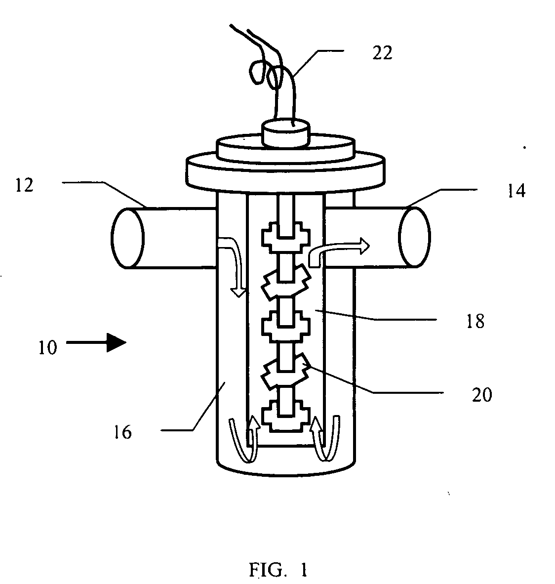
[0026] As noted above, the accumulation of by-products from a semiconductor manufacturing process, in the apparatus components of the processing system can cause equipment failure and also may require system shut-down to clean the components, resulting in substantial cost.

[0027] Also as noted, various approaches have been attempted to overcome the problem of by-product accumulation. This includes employing a fore-line trap, which as noted, has not proved to be efficient.

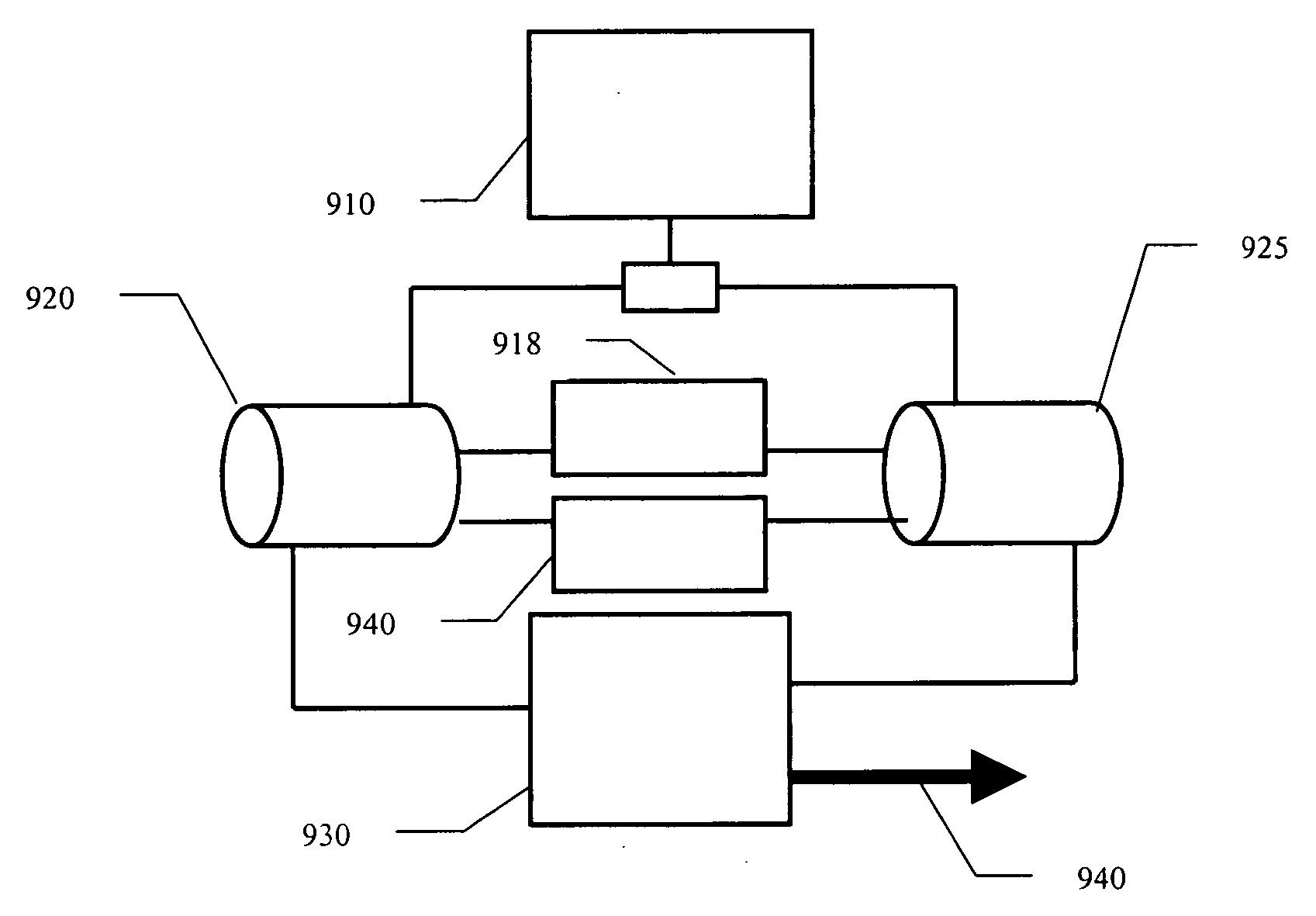
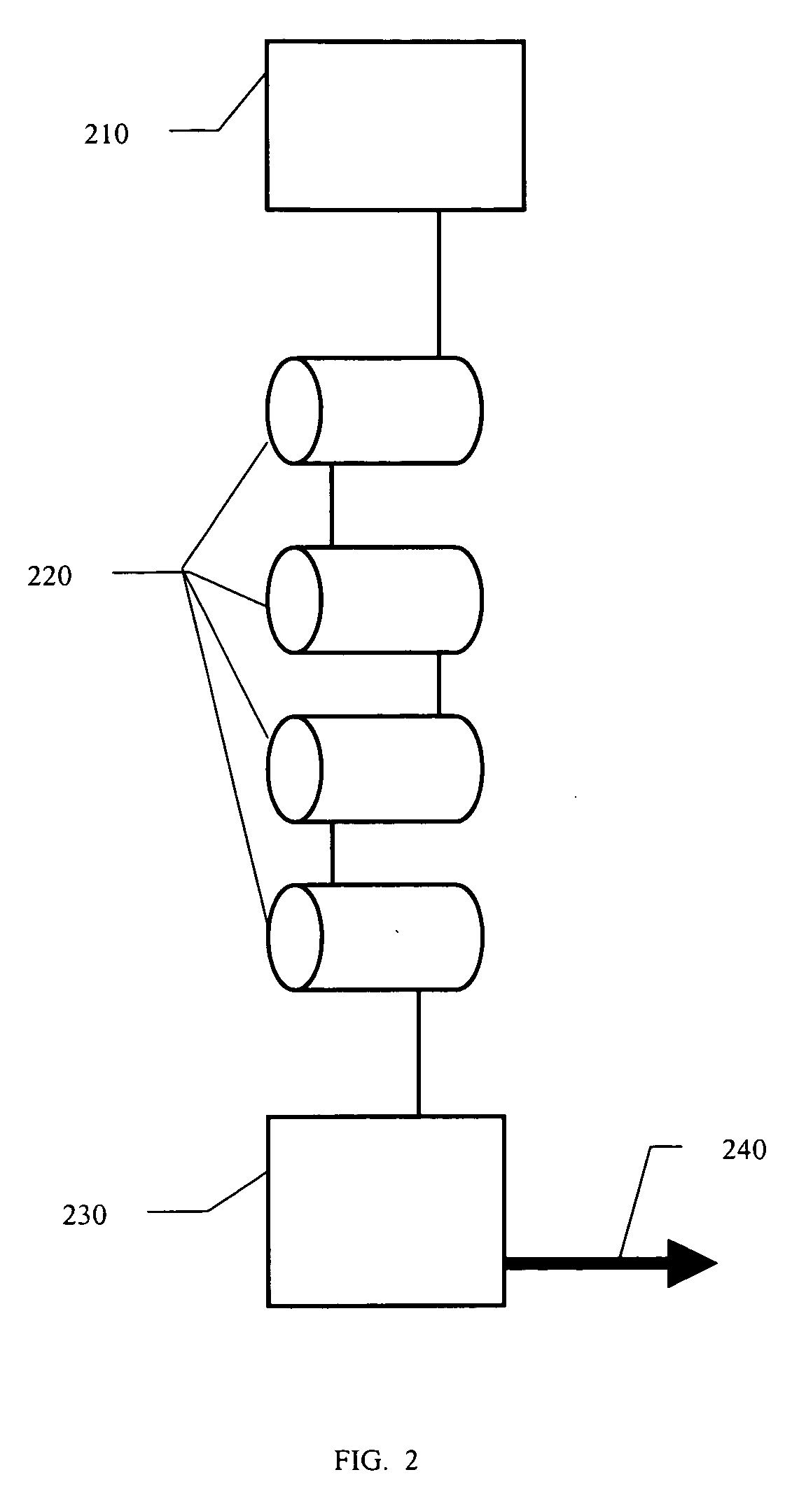
[0028] The present invention solves the problem of fore-line trap inefficiency. In particular, the present invention provides a semiconductor manufacturing system using a fore-line trap that can remove 99% or more of the by-products from the exhaust gas from the processing chamber. I addition, the present invention provides for means to clean the trap of accumulated by-products without requiring shut-down of the deposition system, resulting in significant cost savings. The present invention will be described in gre...


PUM

PropertyMeasurementUnit
Fractionaaaaaaaaaa
Fractionaaaaaaaaaa
Fractionaaaaaaaaaa

Abstract

The present invention provides a system, apparatus and method for improving the efficiency of a semiconductor processing system, such as a deposition system by decreasing or substantially eliminating the accumulation of by-products in the apparatus components of the semiconductor processing system. The present invention further relates to improving the efficiency of a foreline trap associated with a semiconductor processing system, wherein the trap removes substantially all of the by-products from the exhaust gas from the processing chamber. In addition, the present invention provides a system, apparatus and method for efficiently clearing traps of accumulated by-products from exhaust gas of a semiconductor processing system.

Description

FIELD OF THE INVENTION [0001] The present invention relates to new and useful systems, apparatus and methods in the field to semiconductor manufacturing. BACKGROUND OF THE INVENTION [0002] Thin film deposition processes for depositing films of pure and compound materials are known. In recent years, the dominant technique for thin film deposition has been chemical vapor deposition (CVD). A variant of CVD, Atomic Layer Deposition (ALD) has been considered to be an improvement in thin layer deposition in terms of uniformity and conformity, especially for low temperature deposition. [0003] Generally, an ALD process comprises a series of conventional CVD processes, each producing a single-monolayer deposition, wherein each deposition step theoretically goes to saturation at a single molecular or atomic monolayer thickness, and then self-terminates. The deposition is the outcome of chemical reactions between reactive molecular precursors delivered to the system and a substrate. The net re...

Claims


Application Information

Patent Timeline
IPC IPC(8): H01L21/31H01L21/306C23C16/00
CPCC23C16/4412
Inventor BAILEY, CHRISTOPHER M.HOGLE, RICHARDSEELEY, ANDREW JAMES
Owner EDWARDS VACUUM INC
Why Eureka
Try Eureka