Method for manufacturing nitride-based semiconductor device

a semiconductor and nitride technology, applied in the direction of semiconductor devices, basic electric elements, electrical apparatus, etc., can solve the problems of poor quality of sapphire substrate, inability to manufacture large-scale devices, and large defects in sapphire substrates, etc., to achieve high quality

Inactive Publication Date: 2006-12-14
SAMSUNG ELECTRONICS CO LTD
View PDF7 Cites 41 Cited by
  • Summary
  • Abstract
  • Description
  • Claims
  • Application Information

AI Technical Summary

Benefits of technology

[0011] The present invention has been made in view of the above problems, and it is an object according to certain embodiments of the present invention to provide a method for ...

Problems solved by technology

However, the most important problem in terms of growth of GaN-based semiconductors is that a substrate, upon which the GaN-based semiconductor is grown, has yet to be remarkably enhanced in quality.
However, due to lattice mismatch and thermal expansion coefficient differences between the sapphire substrate and the GaN-based semiconductor, the GaN-based semiconductor grown on the sapphire substrate has a negative crystallinity, causing lots of defects in the sapphire substrate.
Additionally, the sapphire substrate is not only relatively expensive, but also inappropriate for large-scale devices....

Method used


Image

  • Method for manufacturing nitride-based semiconductor device
  • Method for manufacturing nitride-based semiconductor device
  • Method for manufacturing nitride-based semiconductor device

Examples


Embodiment Construction

[0024] Preferred embodiments will now be described in detail with reference to the accompanying drawings. It should be noted that the embodiments of the invention can take various forms, and that the present invention is not limited to the embodiments described herein. The embodiments of the invention are -described so as to enable those having an ordinary knowledge in the art to have a better understanding of the invention. Accordingly, shape and size of components of the invention are enlarged in the drawings for clear description of the invention. Like components are indicated by the same reference numerals throughout the drawings.

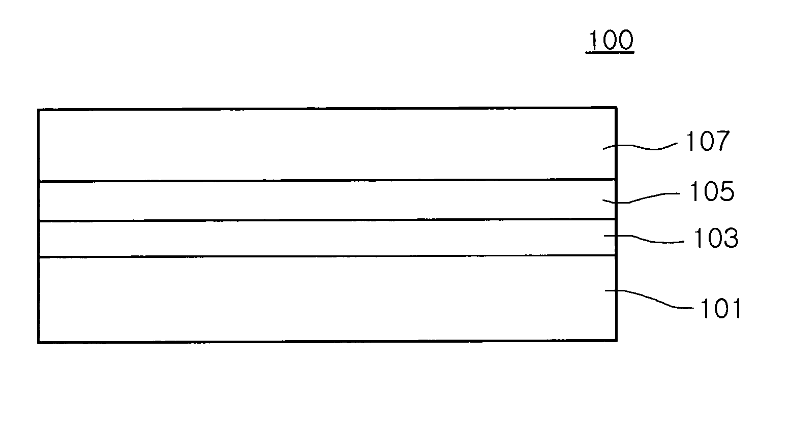
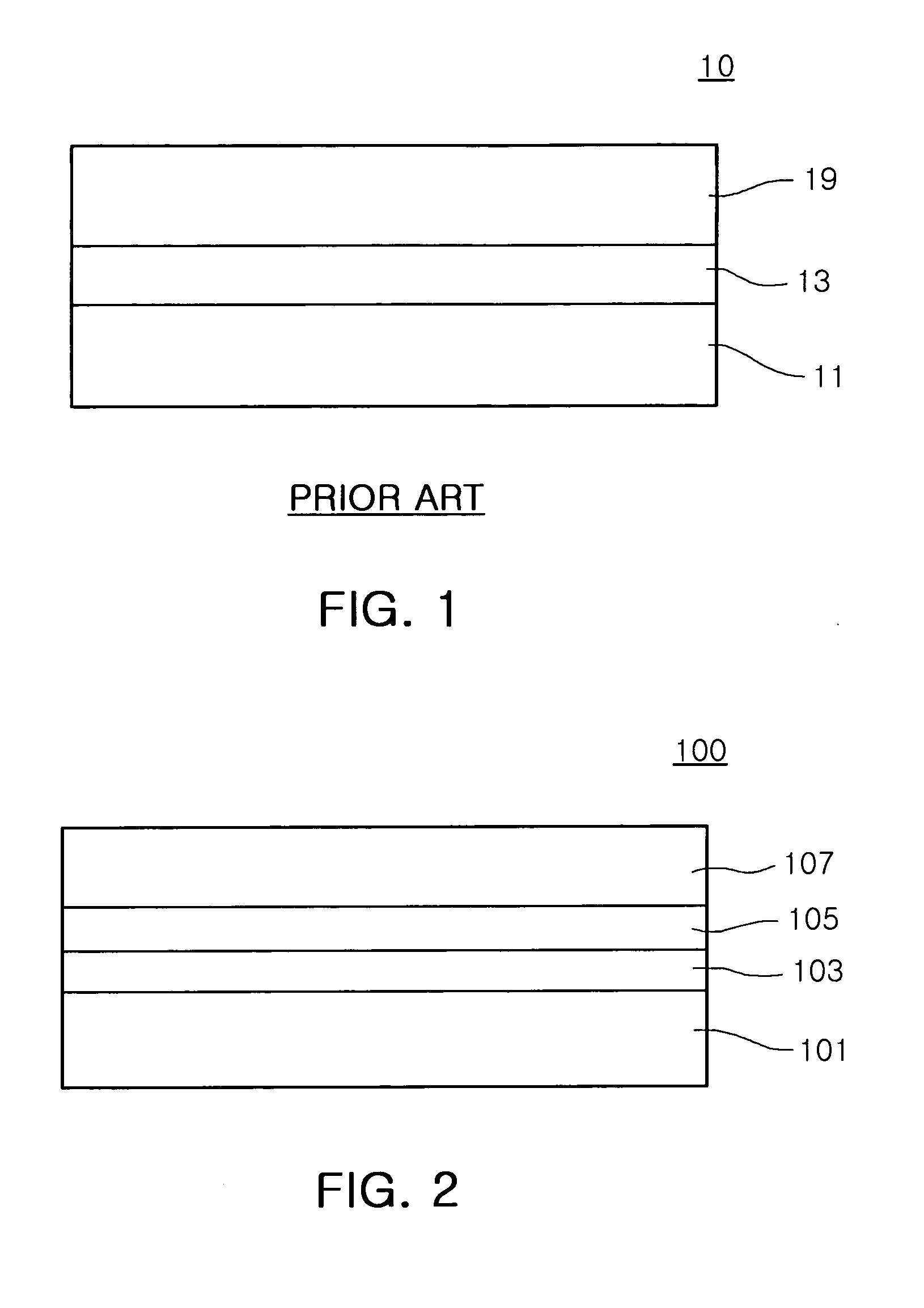
[0025]FIG. 2 is a side sectional view illustrating a nitride-based semiconductor device 100 manufactured according to an embodiment of the invention. Referring to FIG. 2, after an AlN nucleation layer 103 and a GaN buffer layer 105 are sequentially formed on a substrate 101 formed of a different material from the GaN buffer layer 105, a desired GaN-bas...


PUM


Abstract

In a method for manufacturing a high-quality GaN-based semiconductor layer on a substrate of different material, an AlN nucleation layer is grown on a substrate, a GaN buffer layer is grown on the AlN nucleation layer, and the substrate annealed. The AlN nucleation layer is formed to have a thickness greater than a critical radius of a nucleus of AlN crystal and less than a critical resilient thickness of AlN, and the GaN buffer layer is formed to have a thickness greater than a critical radius of a nucleus of GaN crystal and less than a critical resilient thickness of GaN. Annealing time is greater than L2/DGa where L indicates a diffusion distance of Ga, and DGa indicates a diffusion coefficient of Ga in the AlN nucleation layer.

Description

RELATED APPLICATION [0001] The present invention is based on, and claims priority from, Korean Application Number 2005-49985, filed Jun. 10, 2005, the disclosure of which is incorporated by reference herein in its entirety. BACKGROUND OF THE INVENTION [0002] 1. Field of the Invention [0003] The present invention relates to a method for manufacturing a nitride-based semiconductor device, and, more particularly, to a method for manufacturing a GaN-based semiconductor layer on a heterogeneous substrate. [0004] 2. Description of the Related Art [0005] As group III nitride light emitting diodes (LED) employing an AlxInyGa(1−x−y)N-based (where 0≦x≦1, 0≦y≦1, 0≦x+y≦1; which will be referred to as “GaN-based” hereinafter) semiconductor have been developed, GaN semiconductors have been spotlighted as a light source of white, green, or blue light, and many advances have been made in related technology. [0006] However, the most important problem in terms of growth of GaN-based semiconductors is...

Claims


Application Information

Patent Timeline
IPC IPC(8): H01L21/00H01L33/12H01L33/32
CPCH01L21/0237H01L21/02381H01L21/02458H01L21/02502H01L33/12H01L21/0254H01L21/0262H01L33/007H01L21/02513
Inventor PARK, HEE SEOK
Owner SAMSUNG ELECTRONICS CO LTD
Why Eureka
Try Eureka