Method for extracting the distribution of charge stored in a semiconductor device

Active Publication Date: 2006-12-21
INTERUNIVERSITAIR MICRO ELECTRONICS CENT (IMEC VZW)
View PDF4 Cites 7 Cited by
  • Summary
  • Abstract
  • Description
  • Claims
  • Application Information

AI Technical Summary

Benefits of technology

[0012] By performing the varying base-level and the varying top-level charge pumping measurements, not only the spatial charge distribution of charge stored the charge-trapping layer can be extracted, but also the spatial charge distribution of charge stored in interface traps. In this way, the spatial distribution of both electrons and holes in the dielectric layer is obtained. The thus obtained hole and electron distribution curves are used for physical understanding and further optimisation of charge-trapping devices. In particular, the curves can be used to characterize the impact of electrical stress on charge retention character

Problems solved by technology

However, poor endurance and poor retention after cycling, i.e. repetitive programming and erasing of a cell, are major drawbacks of NROM™.
Currently the exact cause of the poor endurance and poor charge retention properties of non-volatile charge-trapping memory devices, in particular of NROM™ devices, is not yet known, impeding the improvement of these properties.
Although this measurement procedure allows extracting the lateral distribution of electrons injected in the device during a programming step, it doesn't take into account the variation of the density of charge traps present at the interface between the channel and the dielectric stack and assumes this density to be uniform along the channel.
Moreover when the device is subjected to multi

Method used


Image

  • Method for extracting the distribution of charge stored in a semiconductor device
  • Method for extracting the distribution of charge stored in a semiconductor device
  • Method for extracting the distribution of charge stored in a semiconductor device

Examples


Embodiment Construction

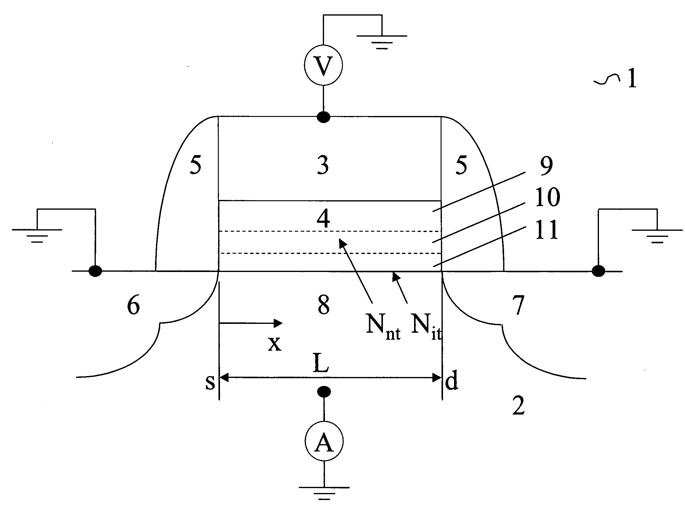
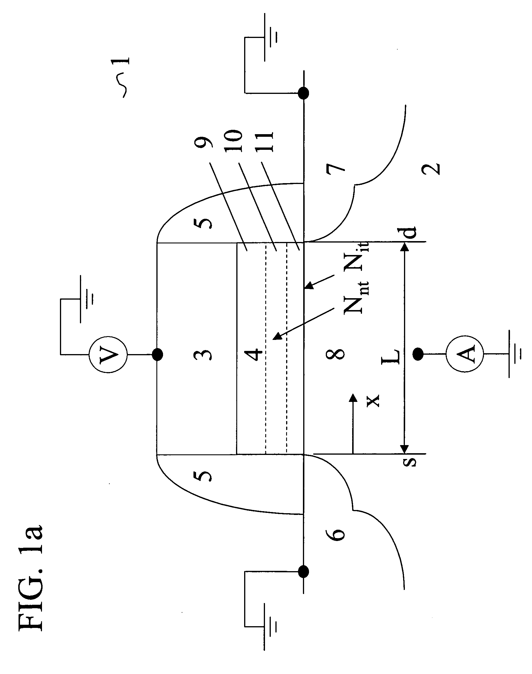
[0025]FIG. 1 shows a schematic cross-section of a MOSFET-type device. This device (1) comprises a gate electrode (3) separated from the substrate (2) by a gate dielectric (4). Typically the gate electrode is formed from a semiconductor material such as polycrystalline silicon doped to obtain the desired workfunction and / or conductivity. This semiconductor material can be partially or fully silicided as known in the art or even metals, e.g. Al, TiN, TaN, are used. The gate dielectric (8) comprises a dielectric charge-trapping layer (10) such as silicon-nitride, silicon-rich oxide, silicon-oxynitride, an oxide layer comprising nanocrystals of a semiconductor material, e.g. polycrystalline silicon. Optionally this charge-trapping layer can be separated from the substrate (2) by another dielectric layer (11) with low or no trapping capabilities, e.g. silicon-oxide. Another layer (9) in a similar material as layer (11) can be used to separate the charge-trapping layer (10) from the gate ...


PUM


Abstract

A method is described for extracting the spatial distribution of charge stored in a charge-trapping layer of a semiconductor device. The method comprises the steps of performing a first charge-pumping measurement on a device under test using a variation of the upper level of the pulse and performing a second charge-pumping measurement on this device using a variation of the lower level of the pulse. The data obtained is combined for extracting the spatial distribution. This is done by establishing a relation between a charge pumping current Icp and a calculated channel length Lcalc of the semiconductor device by reconstructing spatial charge distribution estimates from the charge pumping curves for multiple values of the charge pumping current Icp. From these multiple values of Icp the value is obtained for which the corresponding calculated channel length Lcalc is substantially equal to the effective channel length Leff of the semiconductor device and the spatial charge distribution is reconstructed from the charge pumping curves using the obtained value of Icp.

Description

[0001] This application claims the priority of European Patent Application No. 05109600 (filed Oct. 14, 2005) and Provisional United States Patent Application Nos. 60 / 687,076 (filed Jun. 3, 2005) and 60 / 704,859 (filed Aug. 1, 2005). BACKGROUND [0002] 1. Technical Field [0003] The present invention is in the field of semiconductor processing and devices, more specifically in the field of non-volatile charge-trapping memory devices. In particular, the present invention relates to a method for extracting the spatial distribution of charge stored in a charge-trapping layer of a semiconductor device, according to the preamble of the first claim. [0004] 2. Background Art [0005] Non-volatile memories (NVM) are characterized by the fact that once a bit is stored in a memory cell this bit will be retained even when the memory cell is no longer powered. When electrical fields are used for erasing and programming of the memory cell, the NVM devices are also known as EEPROM (Electrically-Erasab...

Claims


Application Information

Patent Timeline
IPC IPC(8): G01N23/00
CPCG11C16/0475G11C16/3495G11C16/26
Inventor FURNEMONT, ARNAUD ADRIEN
Owner INTERUNIVERSITAIR MICRO ELECTRONICS CENT (IMEC VZW)
Why Eureka
Try Eureka