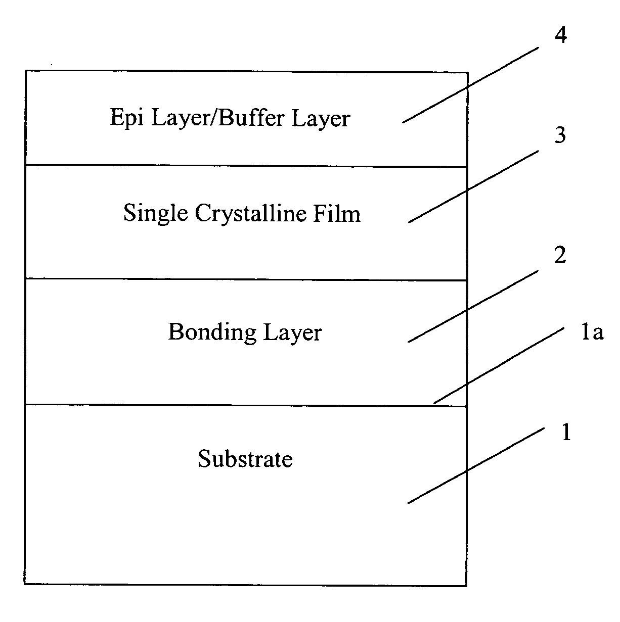
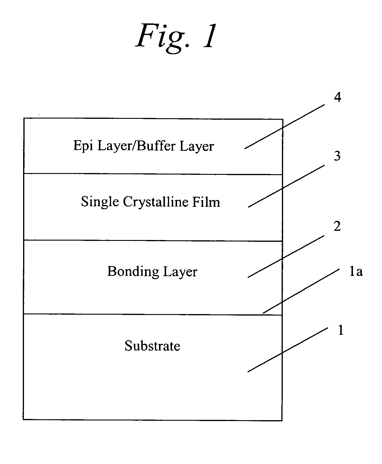
Multilayered substrate obtained via wafer bonding for power applications
a technology of power applications and wafer bonding, applied in the direction of thermoelectric device junction materials, semiconductor devices, electrical apparatus, etc., can solve the problems of limited availability of suitable substrates for epitaxial growth, inability to achieve thermal dissipation properties that are necessary, and prohibitive cost and availability of these wafers
- Summary
- Abstract
- Description
- Claims
- Application Information
AI Technical Summary
Benefits of technology
Problems solved by technology
Method used
Image

Examples
examples
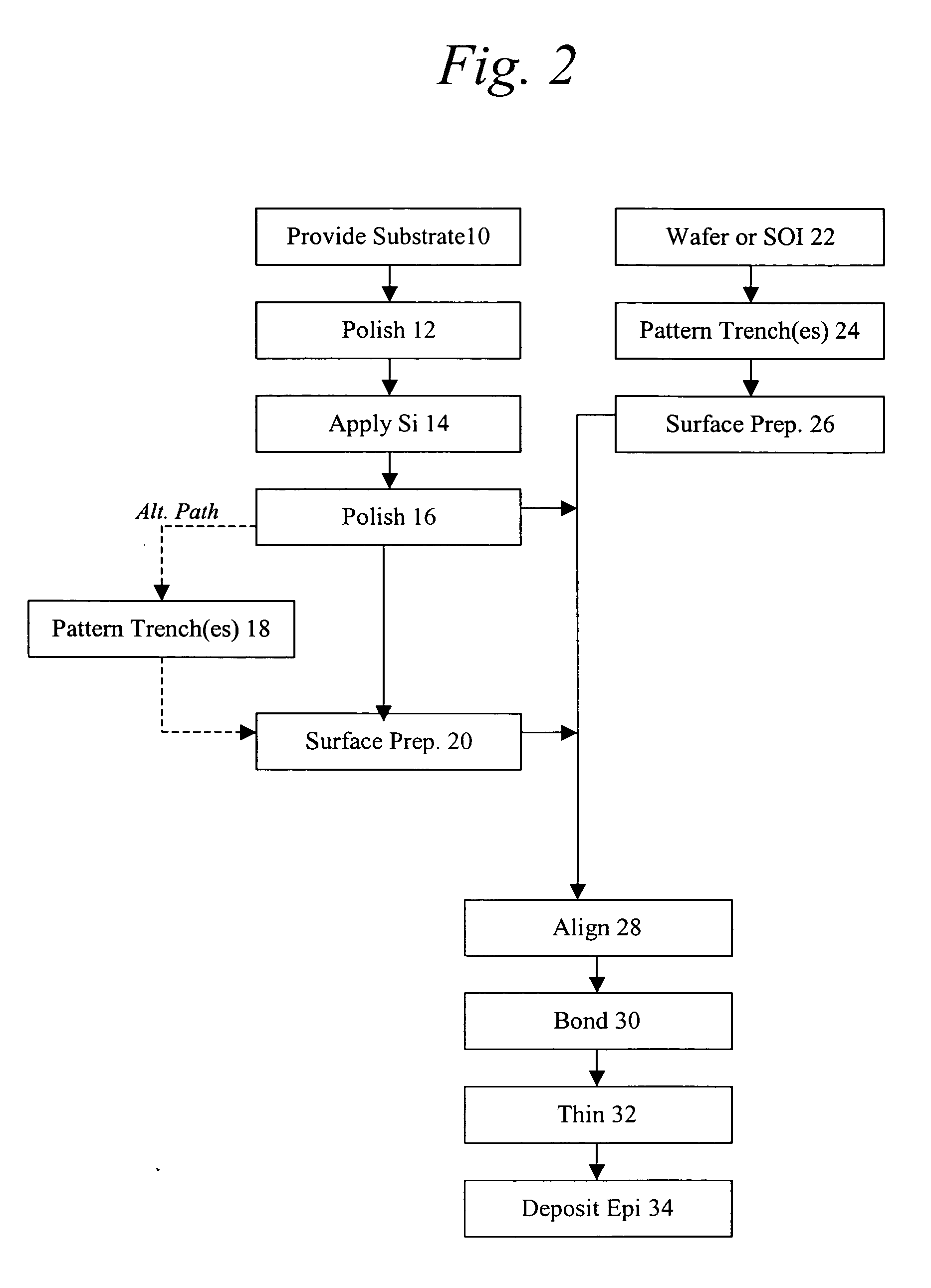
[0087] Two examples demonstrate the successful transfer of silicon to silicon carbide: (1) a silicon layer from a bulk silicon wafer to silicon carbide, and (2) a silicon layer from SOI to silicon carbide. Sonoscan images of the two are shown in FIGS. 16a and 16b. Bulk silicon, which is shown in FIG. 16a, was used for the first attempt in order to test the bonding process using the polished polycrystalline silicon carbide wafers. The center region shows small voids that can be attributed the planarization of the silicon layer. This particular set of wafers was thinned to approximately 100 μm.
[0088] The second example of bonding entailed bonding an SOI wafer to polycrystalline silicon carbide. The sonoscan in FIG. 16b shows a uniform bond without voids. This wafer was annealed at 175° C. and thinned to the buried oxide layer. FIG. 17 shows a cross-section of the wafer pair shown in FIG. 16b. In FIG. 17, several layers can be distinguished: the polycrystalline silicon carbide substra...
PUM
| Property | Measurement | Unit |
|---|---|---|
| surface roughness | aaaaa | aaaaa |
| temperature | aaaaa | aaaaa |
| sizes | aaaaa | aaaaa |
Abstract
Description
Claims
Application Information
 - R&D
- Intellectual Property
- Life Sciences
- Materials
- Tech Scout
- Unparalleled Data Quality
- Higher Quality Content
- 60% Fewer Hallucinations
Browse by: Latest US Patents, China's latest patents, Technical Efficacy Thesaurus, Application Domain, Technology Topic, Popular Technical Reports.
© 2025 PatSnap. All rights reserved.Legal|Privacy policy|Modern Slavery Act Transparency Statement|Sitemap|About US| Contact US: help@patsnap.com