Thin film fuse phase change cell with thermal isolation layer and manufacturing method

a phase change cell and thermal isolation layer technology, applied in the direction of digital storage, semiconductor devices, instruments, etc., can solve the problems of slowing down the heating effect of current, one problem associated with the small dimensions of phase change cells, etc., to achieve low power consumption, small reset current, and simple structure

Active Publication Date: 2006-12-21
MACRONIX INT CO LTD
View PDF99 Cites 212 Cited by
  • Summary
  • Abstract
  • Description
  • Claims
  • Application Information

AI Technical Summary

Benefits of technology

[0013] The volume of memory material subject of phase change can be very small, determined by the thickness of the insulating member (path length in the x-direction), the thickness of the thin film used to form the bridge (y-direction), and the width of the bridge orthogonal to the path length (z-direction). The thickness of the insulating member and the thickness of the thin film of memory material used to form the bridge are determined in embodiments of the technology by thin film thicknesses which are not limited by the two graphic processes used in manufacturing the memory cell. The width of the bridge is also smaller than a minimum feature size F that is specified for a lithographic process used in patterning the layer of material in embodiments of the present invention. In one embodiment, the width of the bridge is defined using photoresist trimming technologies in which a mask pattern is used to define a lithographical photoresist structure on the chip having the minimum feature size F, and the photoresist structure is trimmed by isotropic etching to achieve a feature size less than F. The trimmed photoresist structure is then used to lithographically transfer the more narrow pattern onto the layer of memory material. Also, other techniques can be used to form narrow lines of material in a layer on an integrated circuit. Accordingly, a phase change memory cell with simple structure achieves very small reset current and low power consumption, and is easily manufactured.

Problems solved by technology

Problems have arisen in manufacturing such devices with very small dimensions, and with variations in process that meet tight specifications needed for large-scale memory devices.
One problem associated with the small dimensions of phase change cells has arisen because of the thermal conductivity of materials surrounding the active region.
However, heat generated by the current through the material is conducted away by surrounding structures.
This conduction of heat away from the active region in the phase change material slows down the heating effect of the current and interferes with the operation to change the phase.

Method used


Image

  • Thin film fuse phase change cell with thermal isolation layer and manufacturing method
  • Thin film fuse phase change cell with thermal isolation layer and manufacturing method
  • Thin film fuse phase change cell with thermal isolation layer and manufacturing method

Examples


Embodiment Construction

[0035] A detailed description of thin film fuse phase change memory cells, arrays of such memory cells, and methods for manufacturing such memory cells, is provided with reference to FIGS. 1-16.

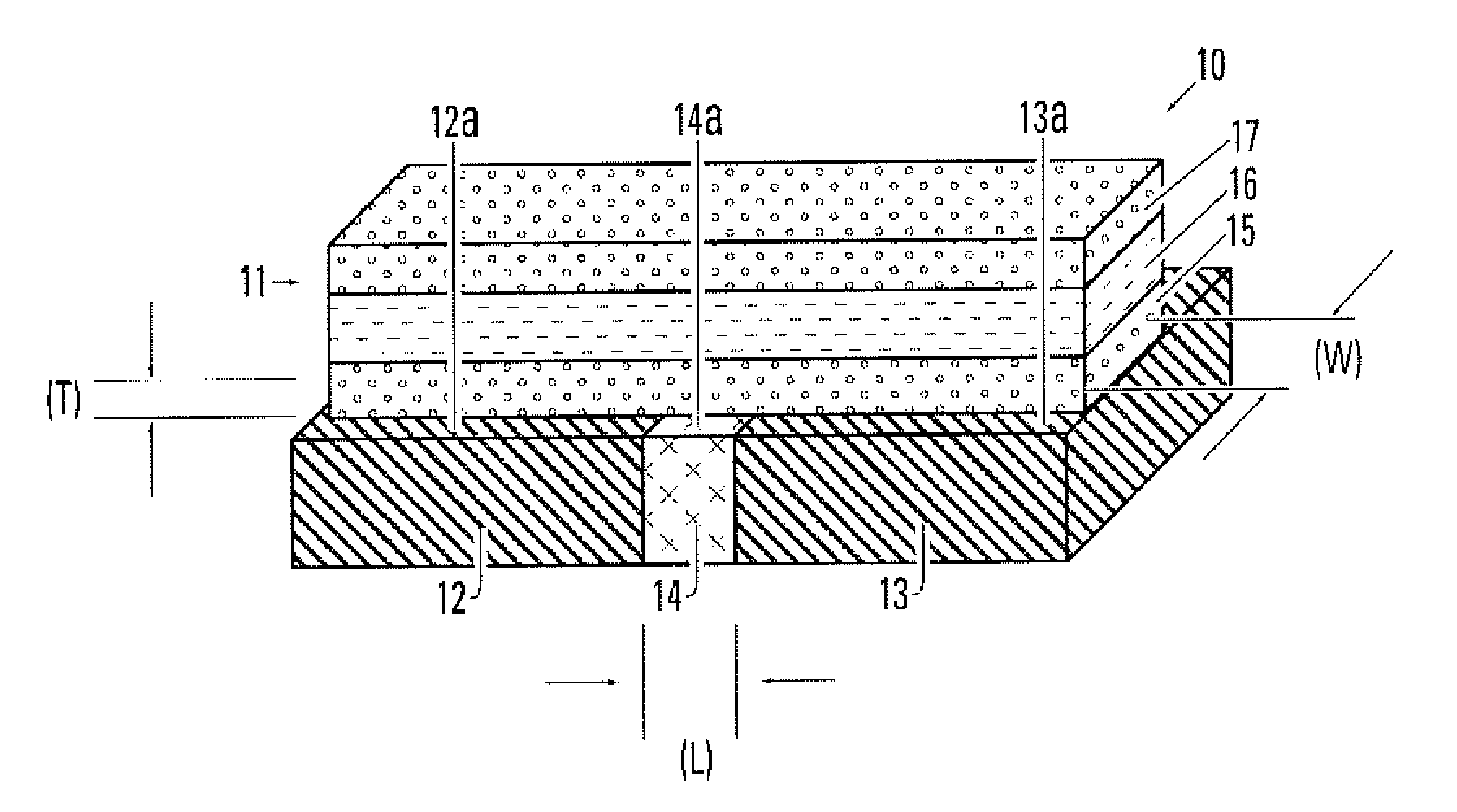
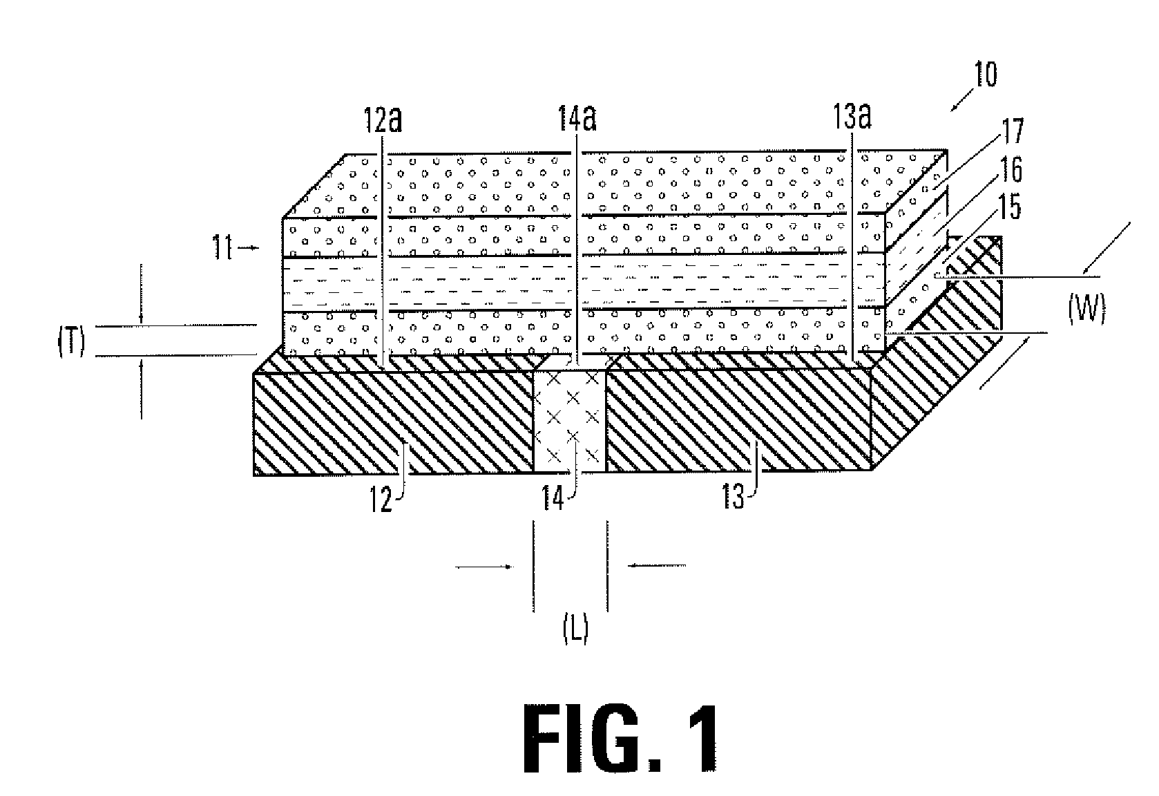
[0036]FIG. 1 illustrates a basic structure of a memory cell 10 including a bridge 11 of memory material on an electrode layer which comprises a first electrode 12, a second electrode 13, and an insulating member 14 between the first electrode 12 and the second electrode 13. As illustrated, the first and second electrodes 12, 13 have top surfaces 12a and 13a. Likewise the insulating member 14 has a top surface 14a. The top surfaces 12a, 13a, 14a of the structures in the electrode layer define a substantially planar top surface for the electrode layer in the illustrated embodiment. In other embodiments, top surfaces 12a, 14a and 13a are not co-planar, with the insulating member 14 extending up forming an insulating wall between the electrodes, for example. The bridge 11 of memory material incl...


PUM


Abstract

A memory device comprising a first electrode having a top side, a second electrode having a top side and an insulating member between the first electrode and the second electrode. The insulating member has a thickness between the first and second electrodes near the top side of the first electrode and the top side of the second electrode. A bridge of memory material crosses the insulating member, and defines an inter-electrode path between the first and second electrodes across the insulating member. An array of such memory cells is provided. The bridge comprises an active layer of memory material on the first side having at least two solid phases and a blanket of thermal insulating material overlying the memory material having thermal conductivity less than that of an overlying electrically insulating layer.

Description

RELATED APPLICATION DATA [0001] The present application is a continuation-in-part of U.S. patent application Ser. No. 11 / 155,067; filed 17 Jun. 2005, which is incorporated by reference as if fully set forth herein.PARTIES TO A JOINT RESEARCH AGREEMENT [0002] International Business Machines Corporation, a New York corporation; Macronix International Corporation, Ltd., a Taiwan corporation, and Infineon Technologies A.G., a German corporation, are parties to a Joint Research Agreement. BACKGROUND OF THE INVENTION [0003] 1. Field of the Invention [0004] The present invention relates to high density memory devices based on phase change based memory materials, including chalcogenide based materials and other materials, and to methods for manufacturing such devices. [0005] 2. Description of Related Art [0006] Phase change based memory materials are widely used in read-write optical disks. These materials have at least two solid phases, including for example a generally amorphous solid pha...

Claims


Application Information

Patent Timeline
Patent Type & Authority Applications(United States)
IPC IPC(8): H01L29/76
CPCG11C13/0004H01L27/2436H01L45/06H01L45/1675H01L45/1293H01L45/144H01L45/148H01L45/1226H10B63/30H10B63/80H10N70/823H10N70/231H10N70/8616H10N70/884H10N70/8828H10N70/063
Inventor CHEN, SHIH HUNG
Owner MACRONIX INT CO LTD
Why Eureka
Try Eureka