

Semiconductor device and method for fabricating the same
a semiconductor device and semiconductor technology, applied in the direction of semiconductor devices, capacitors, electrical equipment, etc., can solve the problems of increasing current, difficult to secure the capacitance required by the highly integrated semiconductor device, and limitation in increasing the effective surface area, so as to increase the effective surface area of the capacitor and secure the capacitan
- Summary
- Abstract
- Description
- Claims
- Application Information
AI Technical Summary
Benefits of technology
Problems solved by technology
Method used
Image

Examples
Embodiment Construction
[0027] Hereinafter, detailed descriptions on certain embodiments of the present invention will be provided with reference to the accompanying drawings.
[0028]FIGS. 3A to 3F are cross-sectional views illustrating a method for fabricating a three dimensional type capacitor in accordance with a first embodiment of the present invention. Herein, among reference numerals illustrated in FIGS. 3A to 3F, the same reference numerals denote the same constitution elements serving the same roles throughout FIGS. 3A to 3F.
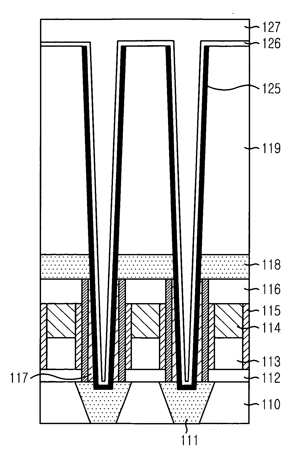
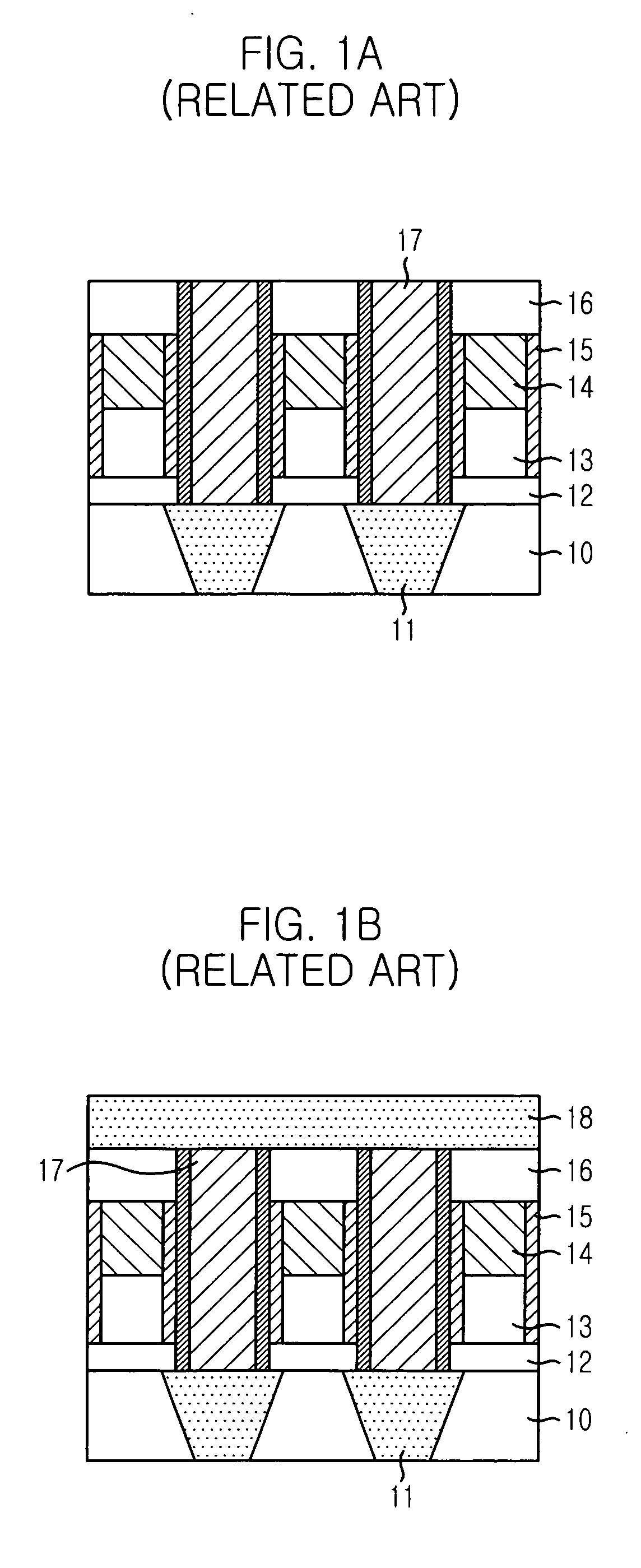
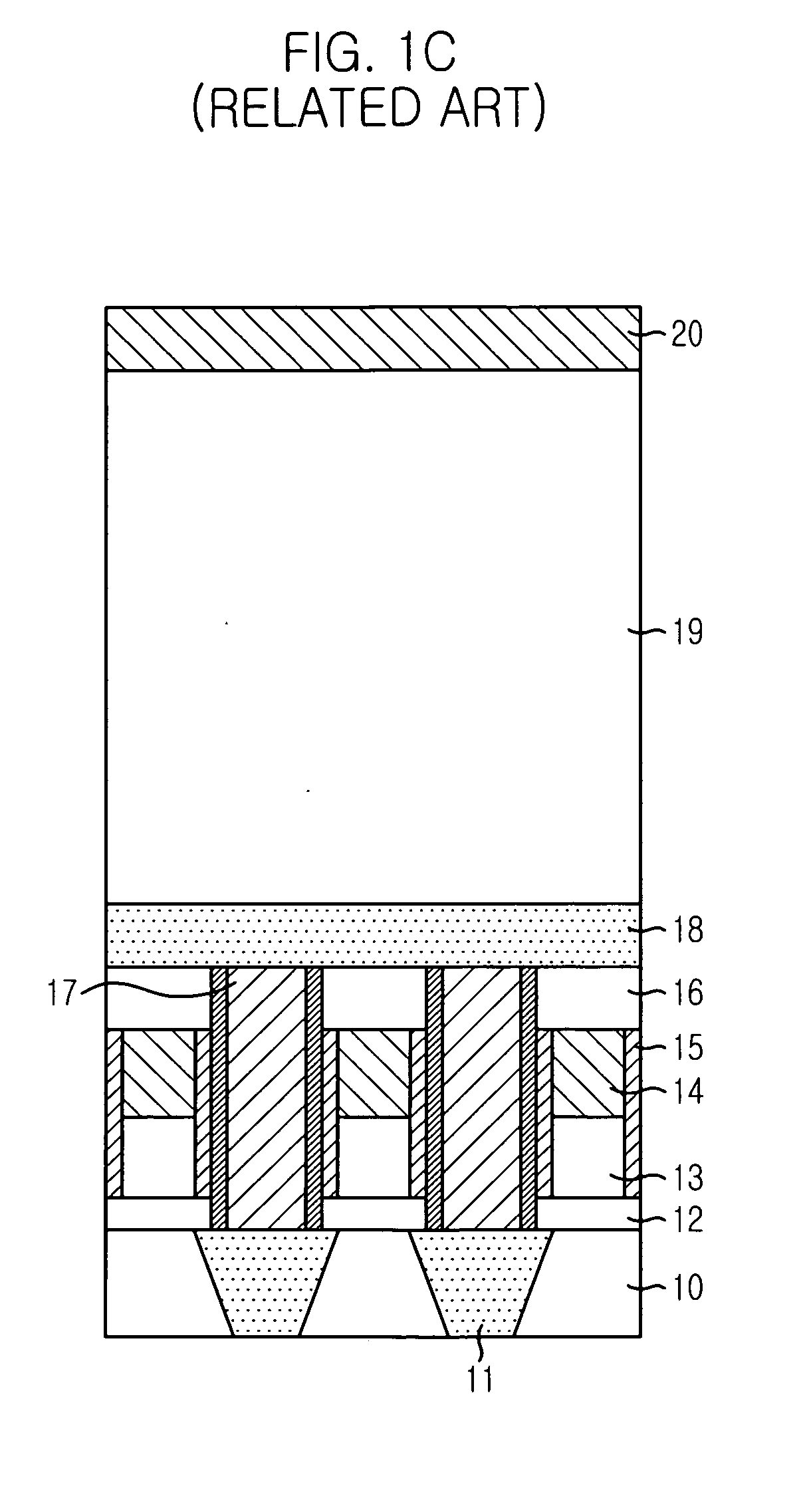
[0029] First, as shown in FIG. 3A, a first insulation layer 110 in which a plurality of first contact layers 111 are interposed in the first insulation layer 110 is formed over a substrate (not shown) provided with a predetermined lower layer (not shown). Herein, the lower layer may include word lines, metal lines and metal plugs. Furthermore, the first insulation layer 110 is formed by using one selected from the group consisting of a high density plasma (HDP) oxide layer, a ...
PUM
 Abstract
Description
Claims
Application Information