

Method for fabricating semiconductor device and semiconductor device
- Summary
- Abstract
- Description
- Claims
- Application Information
AI Technical Summary
Benefits of technology
Problems solved by technology
Method used
Image

Examples
embodiment 1
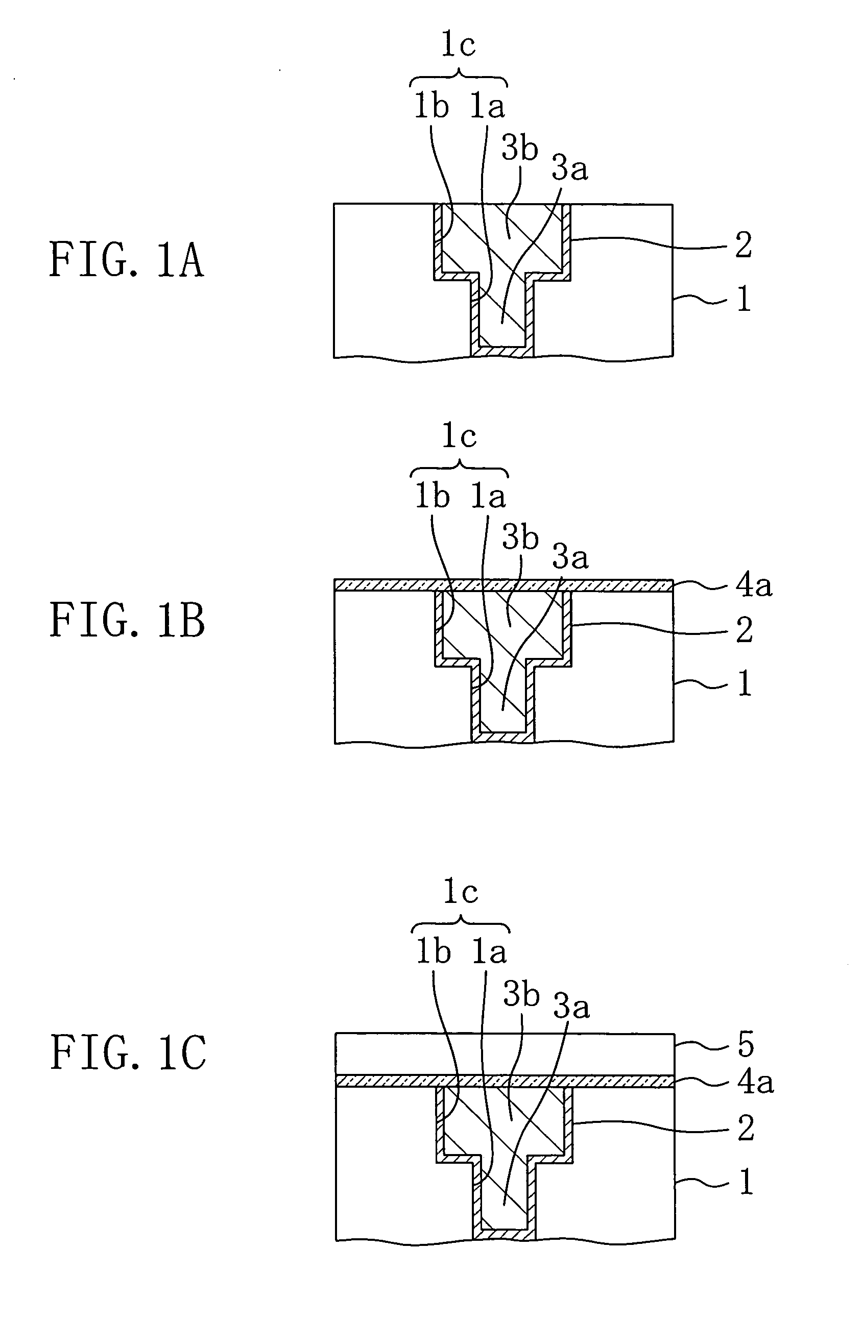
[0034] A method for fabricating a semiconductor device according to Embodiment 1 of the invention will now be described with reference to the accompanying drawings.
[0035]FIGS. 1A through 1C are cross-sectional views for showing procedures in the method for fabricating a semiconductor device of Embodiment 1.
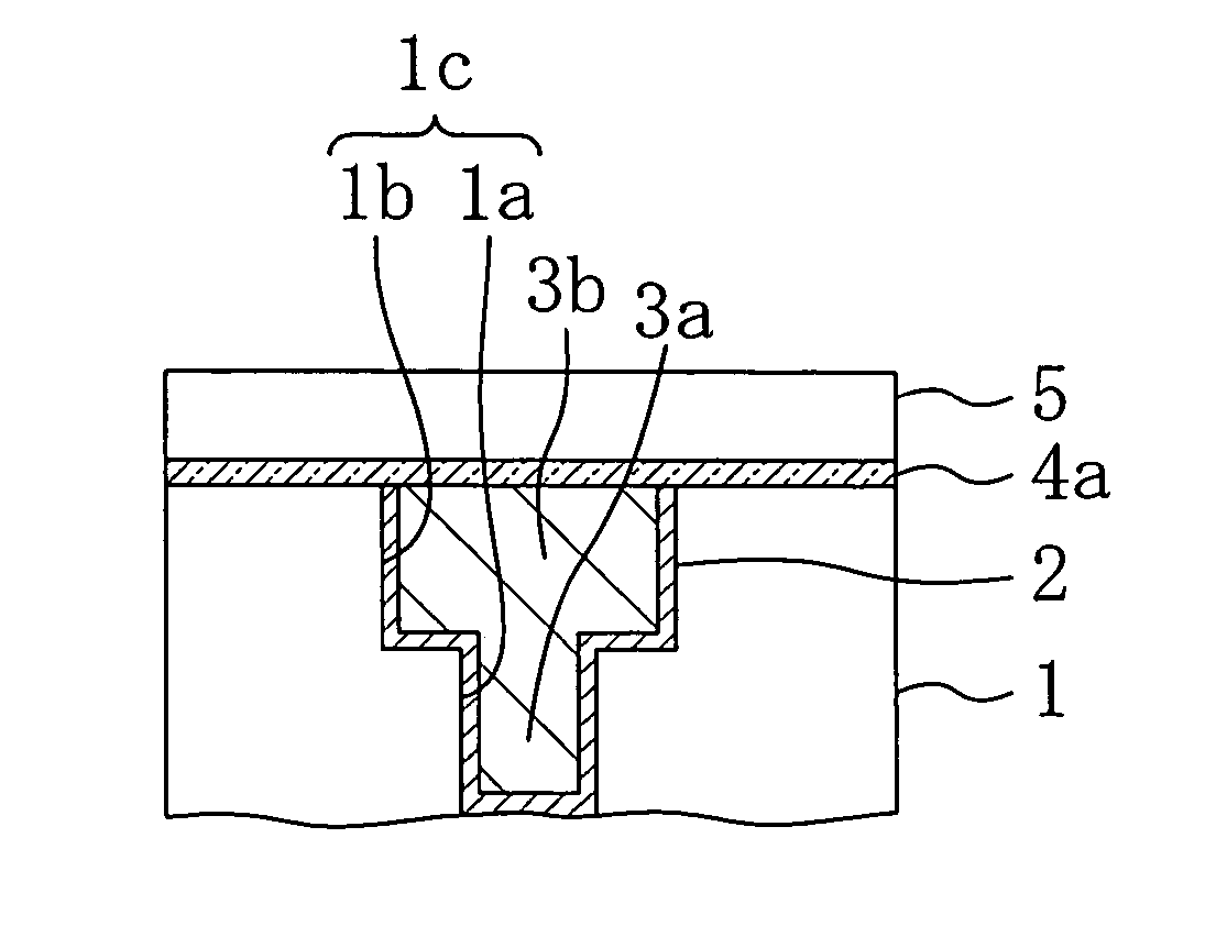
[0036] First, as shown in FIG. 1A, a recess 1c corresponding to a dual damascene interconnect groove composed of a via hole 1a and an interconnect groove 1b communicated with the via hole 1a is formed in a first interlayer insulating film 1 formed on a semiconductor substrate not shown and made of a low dielectric constant material (a low-k material). Thereafter, a barrier film 2 is formed on the inner wall and the bottom of the recess 1c, so as to prevent the first interlayer insulating film 1 from being in direct contact with an interconnect plug 3a and a copper interconnect 3b described below. Then, copper is filled in the recess 1c where the barrier film 2 has been formed an...
embodiment 2
[0046] A method for fabricating a semiconductor device according to Embodiment 2 of the invention will now be described with reference to the accompanying drawings.
[0047]FIGS. 3A through 3C are cross-sectional views for showing procedures in the method for fabricating a semiconductor device of Embodiment 2.
[0048] First, as shown in FIG. 3A, a recess 1c corresponding to a dual damascene interconnect groove composed of a via hole 1a and an interconnect groove 1b communicated with the via hole 1a is formed in a first interlayer insulating film 1 formed on a semiconductor substrate not shown and made of a low dielectric constant material (a low-k material). Thereafter, a barrier film 2 is formed on the inner wall and the bottom of the recess 1c so as to prevent the first interlayer insulating film 1 from being in direct contact with an interconnect plug 3a and a copper interconnect 3b described below. Then, copper is filled within the recess 1c where the barrier film 2 has been formed...
embodiment 3
[0053] A method for fabricating a semiconductor device according to Embodiment 3 of the invention will now be described with reference to the accompanying drawings.
[0054]FIGS. 4A through 4C are cross-sectional views for showing procedures in the method for fabricating a semiconductor device of Embodiment 3.
[0055] First, as shown in FIG. 4A, a recess 1c corresponding to a dual damascene interconnect groove composed of a via hole 1a and an interconnect groove 1b communicated with the via hole 1a is formed in a first interlayer insulating film 1 formed on a semiconductor substrate not shown and made of a low dielectric constant material (a low-k material). Thereafter, a barrier film 2 is formed on the inner wall and the bottom of the recess 1c, so as to prevent the first interlayer insulating film 1 from being in direct contact with an interconnect plug 3a and a copper interconnect 3b described below. Then, copper is filled within the recess 1c where the barrier film 2 has been forme...
PUM
 Abstract
Description
Claims
Application Information