CMOS on SOI substrates with hybrid crystal orientations

Active Publication Date: 2006-12-28
TAIWAN SEMICON MFG CO LTD
View PDF25 Cites 77 Cited by
  • Summary
  • Abstract
  • Description
  • Claims
  • Application Information

AI Technical Summary

Benefits of technology

[0016] For example, in an embodiment of the invention, the epitaxial semiconductor layer comprises (100) silicon on which a PMOS is formed. The second semiconductor layer comprises (110) silicon on which an NMOS is formed. In another embodiment, the epitaxial semiconduct

Problems solved by technology

This, however, is not the optimum CMOS configuration because electrons have their greatest mobility in the {100} family of planes, while holes have their greatest mobility in the {110} family of planes.
Consequently, one type of device is frequently fabricated with the optimum crystal orientation, while the other type of device functions with less than optimal carrier mobility.
Many problems encountered in CMOS fabrication

Method used


Image

  • CMOS on SOI substrates with hybrid crystal orientations
  • CMOS on SOI substrates with hybrid crystal orientations
  • CMOS on SOI substrates with hybrid crystal orientations

Examples


Example

[0026] Corresponding numerals and symbols in different figures generally refer to corresponding parts unless otherwise indicated. The figures are drawn to clearly illustrate the relevant aspects of the preferred embodiments and are not necessarily drawn to scale. To more clearly illustrate certain embodiments, a letter indicating variations of the same structure, material, or process step may follow a figure number.

DETAILED DESCRIPTION OF ILLUSTRATIVE EMBODIMENTS

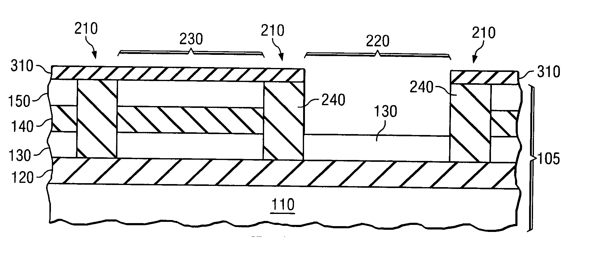
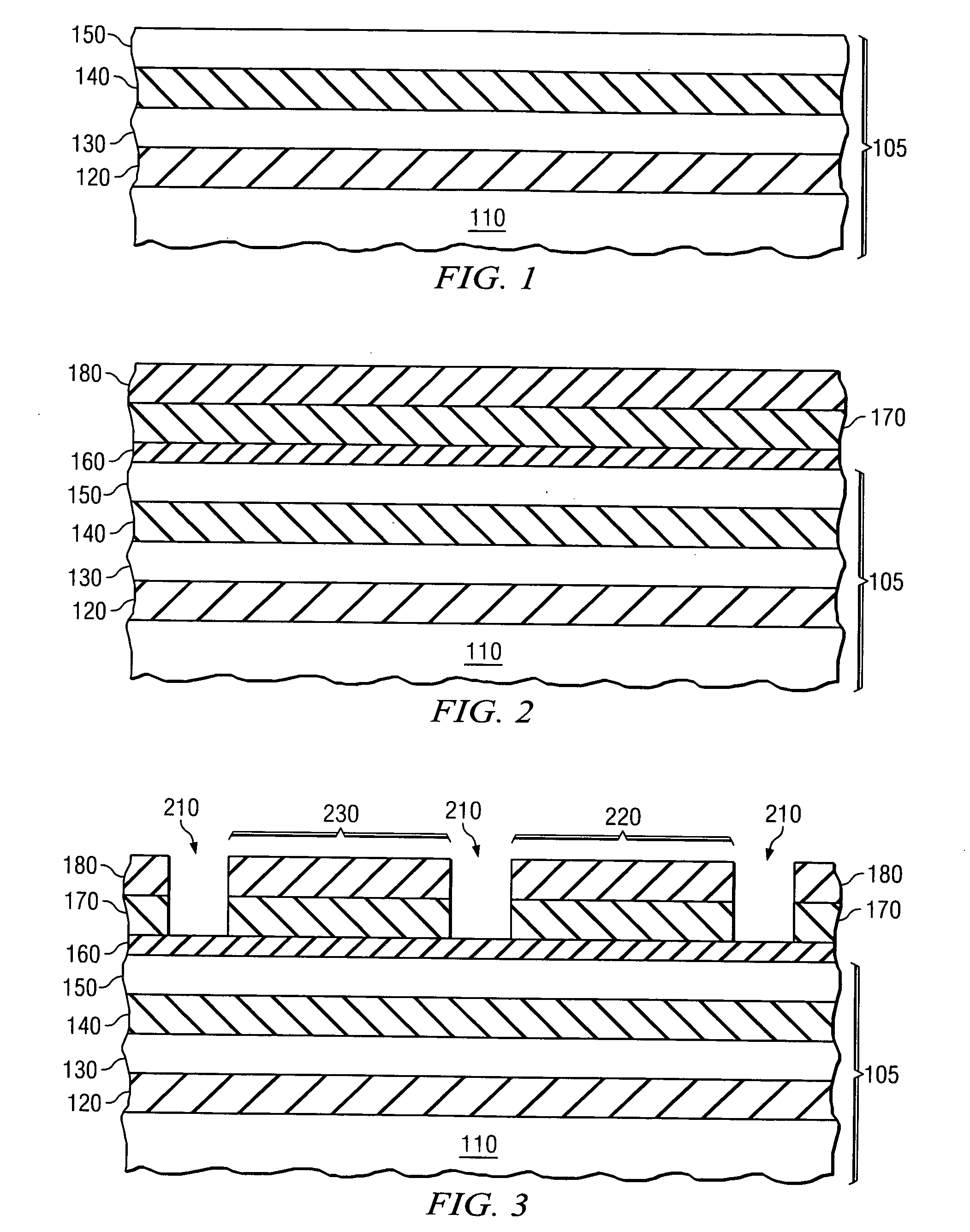
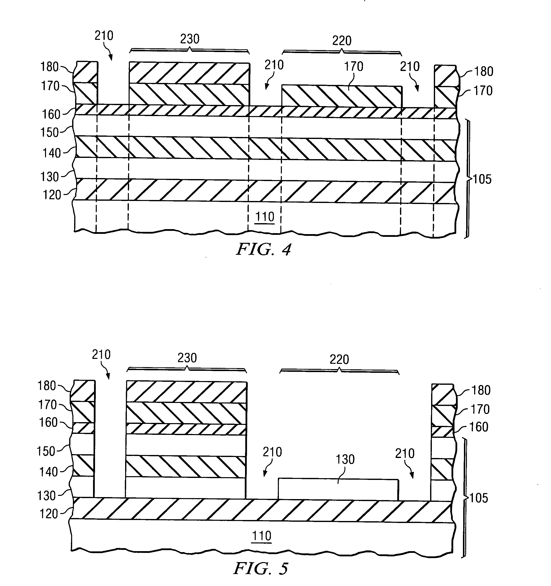
[0027] The making and using of the presently preferred embodiments are discussed in detail below. It should be appreciated, however, that the present invention provides many applicable inventive concepts that may be embodied in a wide variety of specific contexts. The specific embodiments discussed are merely illustrative of specific ways to make and use the invention, and do not limit the scope of the invention.

[0028] The present invention will be described with respect to preferred embodiments in a specific context, nam...


PUM


Abstract

Methods and structures for CMOS devices with hybrid crystal orientations using double SOI substrates is provided. In accordance with preferred embodiments, a manufacturing sequence includes the steps of forming an SOI silicon epitaxy layer after the step of forming shallow trench isolation regions. The preferred sequence allows hybrid SOI CMOS fabrication without encountering problems caused by forming STI regions after epitaxy. A preferred device includes an NFET on a {100} crystal orientation and a PFET on a {110} crystal orientation. An NMOS channel may be oriented along the <100> direction, which is the direction of maximum electron mobility for a {100} substrate. A PMOS channel may be oriented along the <110> direction, which is the direction where hole mobility is maximum for a {110} substrate.

Description

[0001] This application claims the benefit of U.S. Provisional Application No. 60 / 693,384 filed on Jun. 23, 2005, entitled “CMOS on SOI Substrates with Hybrid Crystal Orientations,” which application is hereby incorporated by reference in its entirety.TECHNICAL FIELD [0002] This invention relates generally to semiconductor fabrication and more particularly to methods and structures for CMOS fabrication using double SOI substrates and hybrid crystal orientations. BACKGROUND [0003] Conventional silicon-on-insulator (SOI) CMOS devices typically have a thin layer of silicon, also known as the active layer, on an insulator layer such as a buried oxide (BOX) layer. Active devices, such as MOS transistors (MOSFETs), are formed in active regions within the active layer. The size and placement of the active regions are defined by isolation regions, such as shallow trench isolation (STI) regions. Active devices in the active regions are isolated from the substrate by the BOX layer. [0004] Dev...

Claims


Application Information

Patent Timeline
IPC IPC(8): H01L21/337H01L21/8238
CPCH01L21/823807H01L21/84H01L27/1207H01L29/785H01L27/1203H01L21/76283H01L21/76254
Inventor WU, I-LULIN, CHUNG-TELEE, TAN-CHEN
Owner TAIWAN SEMICON MFG CO LTD
Why Eureka
Try Eureka