Ultrathin semiconductor circuit having contact bumps and corresponding production method

a technology of contact bumps and semiconductor circuits, which is applied in the direction of semiconductor devices, semiconductor/solid-state device details, electrical apparatus, etc., can solve the problems of increased wafer breakage, low yield of above-described contact bumps, and non-uniform pressure distribution, so as to improve the mechanical stability of the semiconductor circuit or the multiplicity of semiconductor circuits. , the effect of significantly reducing the breakage of the wafer

Inactive Publication Date: 2006-12-28
INFINEON TECH AG
View PDF11 Cites 6 Cited by
  • Summary
  • Abstract
  • Description
  • Claims
  • Application Information

AI Technical Summary

Benefits of technology

[0011] According to one embodiment, the limitations of prior solutions are overcome by virtue of the use of a bump supporting layer formed on a surface of a semiconductor circuit. The forces acting on projecting contact bumps during mechanical processing, such as thinning for example, can be made uniform or absorbed, as a result of which a wafer breakage can be significantly reduced and the mechanical stability of the semiconductor circuit or of a semiconductor wafer having a multiplicity of semiconductor circuits can be significantly improved. Moreover, there is an improvement in the adhesive forces between the semiconductor circuit coated with the bump supporting layer and, for example, a molding composition for a component housing as a result of which a so-called delamination is prevented and a moisture resistance is significantly improved. A long-term failure of the packaged semiconductor circuit is thereby significantly reduced.

Problems solved by technology

While semiconductor circuits which are contact-connected according to the wire bonding method have minor problems in this case, the above-described semiconductor circuits with contact bumps exhibit an extremely low yield on account of wafer breakages of the semiconductor wafers.
These low yields result from the contact bumps (on the wafer front side) which project up to 90 micrometers and, during a grinding operation (on the wafer rear side), lead to a nonuniform pressure distribution and thus to an increased wafer breakage.
Additionally, for the concluding adhesive bonding of the semiconductor component to a carrier substrate after soldering, the conventional flip-chip methods exhibit an inadequate moisture resistance and adhesion on the molding composition used for a housing.

Method used


Image

  • Ultrathin semiconductor circuit having contact bumps and corresponding production method
  • Ultrathin semiconductor circuit having contact bumps and corresponding production method
  • Ultrathin semiconductor circuit having contact bumps and corresponding production method

Examples


Embodiment Construction

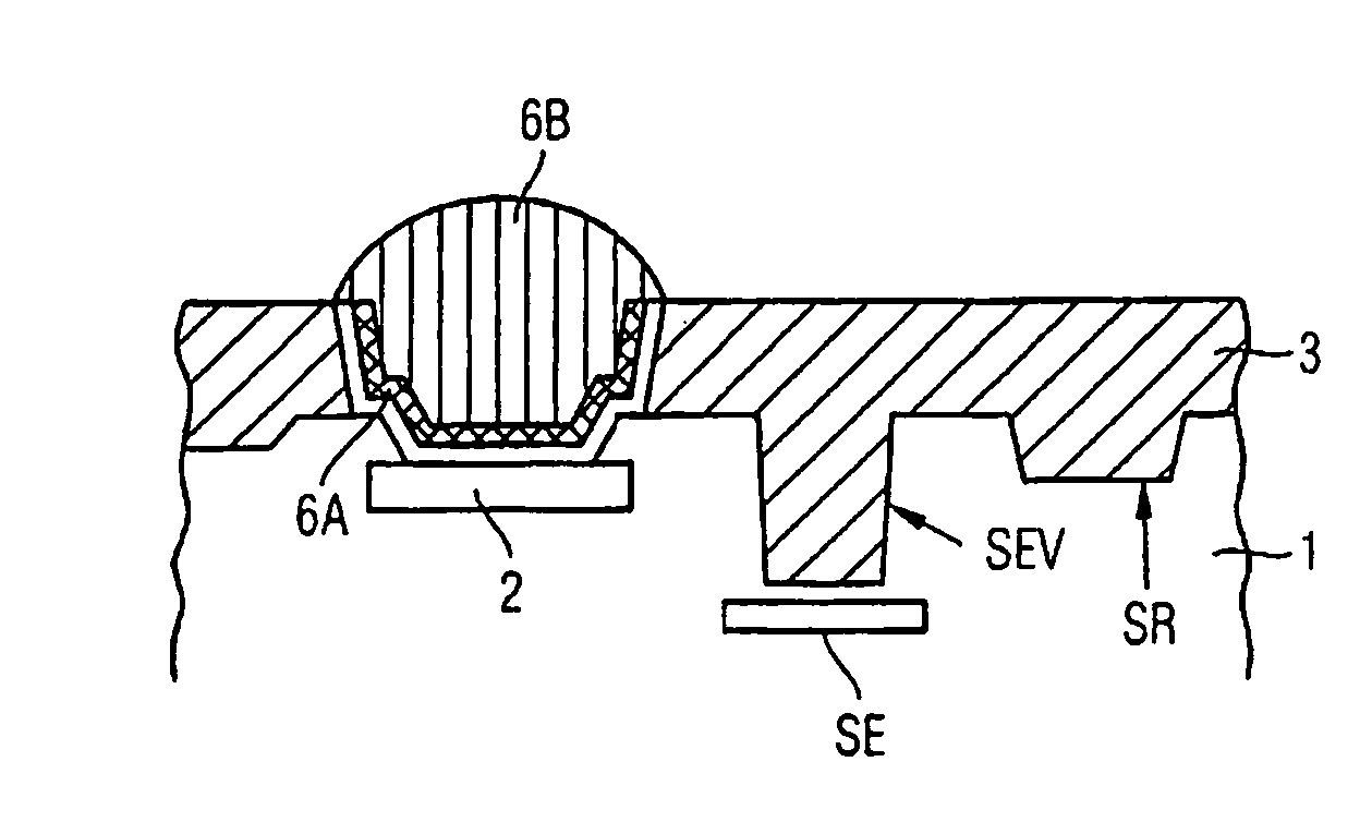
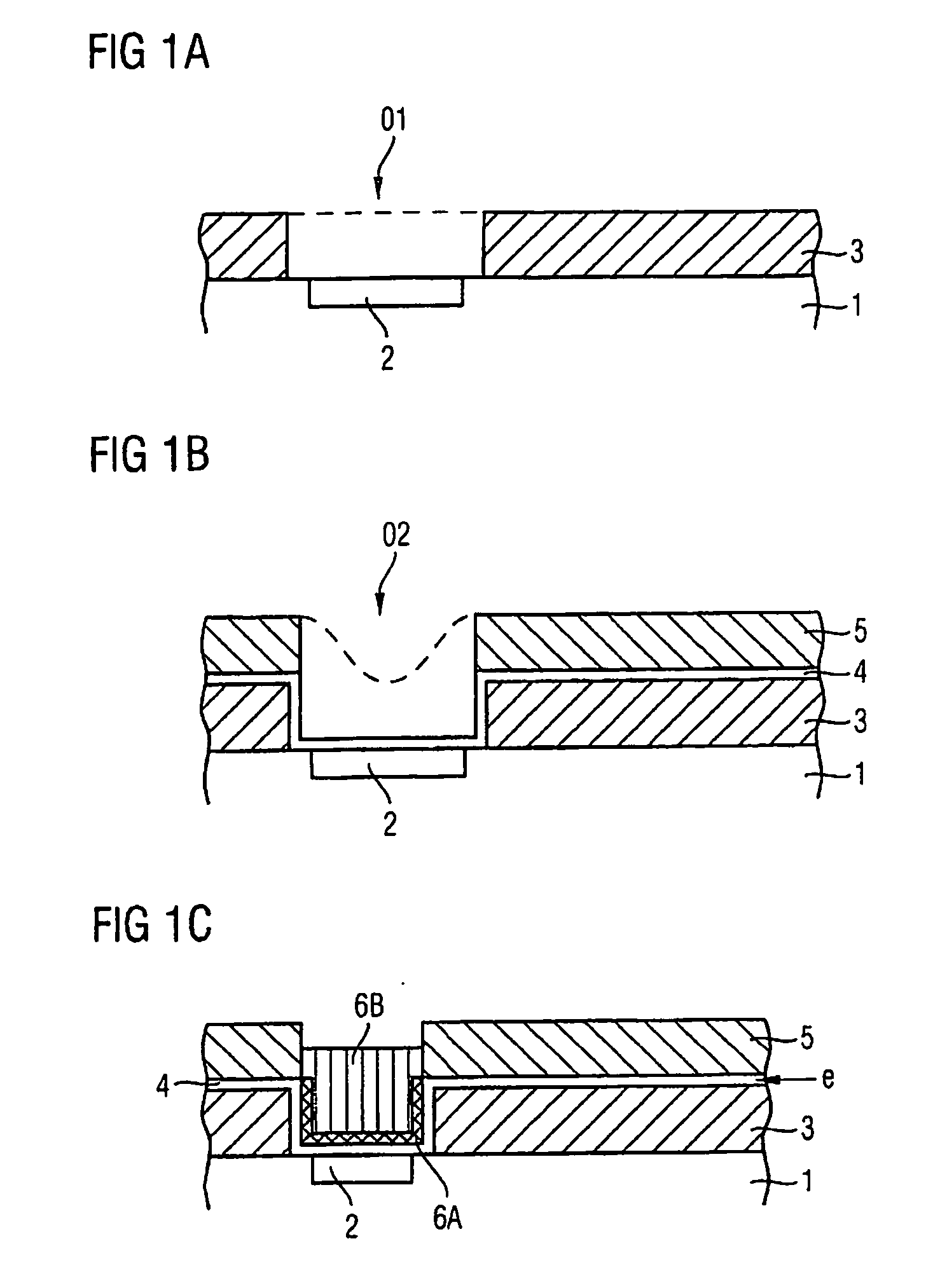
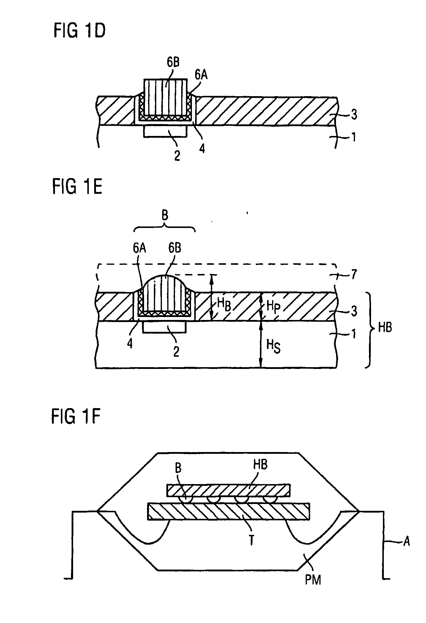
[0018] Referring to FIG. 1A, a contact layer element 2 is formed in the surface of a semiconductor circuit 1, which represents a wiring surface. The contact layer element 2 may represent a so-called Al contact pad in a topmost metallization plane of a wiring layer region. Situated in the underlying layer planes (not illustrated) of the semiconductor circuit 1 or the wiring layer region thereof, there are further metallization planes or insulating intermediate layers, down to a semiconductor substrate in which the actual semiconductor components are realized.

[0019] Silicon is preferably used as semiconductor material. A multiplicity of semiconductor circuits being formed on a semiconductor wafer. Semiconductor wafers of this type initially have a thickness of 700 to 750 micrometers, for which reason they are sufficiently mechanically stable and can thus be handled in a simple manner.

[0020] In order to improve a mechanical stability in particular during a subsequent process of thinn...


PUM


Abstract

The invention relates to an ultrathin semiconductor circuit having contact bumps and to a corresponding production method. The semiconductor circuit includes a bump supporting layer having a supporting layer thickness and having a supporting layer opening for uncovering a contact layer element being formed on the surface of a semiconductor circuit. An electrode layer is situated on the surface of the contact layer element within the opening of the bump supporting layer, on which electrode layer is formed a bump metallization for realizing the contact bump. On account of the bump supporting layer, a thickness of the semiconductor circuit can be thinned to well below 300 micrometers, with the wafer reliably being prevented from breaking. Furthermore, the moisture barrier properties of the semiconductor circuit are thereby improved.

Description

CROSS REFERENCE TO RELATED APPLICATIONS [0001] This application is a continuation of international application PCT / EP2004 / 052258, filed Sep. 21, 2004, which claims priority to German patent application serial number DE 10355508.0, filed Nov. 27, 2003.BACKGROUND [0002] 1. Field of the Invention [0003] The present invention relates to an ultrathin semiconductor circuit having contact bumps and to a corresponding production method. [0004] 2. Description of the Related Art [0005] Semiconductor circuits or semiconductor components are electrically connected to carrier substrates or leadframes by various methods including wire, flip-chip and tape automated bonding methods which represent the most important methods. While in the case of the wire bonding method, the individual connection locations or connection pads on the semiconductor circuit or the semiconductor component are successively connected to the corresponding contact locations on the leadframe by means of fine wires (bonding wi...

Claims


Application Information

Patent Timeline
Patent Type & Authority Applications(United States)
IPC IPC(8): H01L21/44H01L23/48H01L21/60H01L23/00H01L23/485H01L23/525
CPCH01L23/5258H01L23/562H01L24/03H01L24/05H01L24/11H01L24/13H01L2224/0345H01L2224/03462H01L2224/0401H01L2224/05082H01L2224/05147H01L2224/05155H01L2224/05166H01L2224/05571H01L2224/05624H01L2224/05647H01L2224/05655H01L2224/11462H01L2224/1147H01L2224/11849H01L2224/13022H01L2224/13111H01L2224/48247H01L2924/01004H01L2924/01005H01L2924/01006H01L2924/01013H01L2924/01014H01L2924/0102H01L2924/01028H01L2924/01029H01L2924/01032H01L2924/01038H01L2924/0105H01L2924/01052H01L2924/01061H01L2924/01078H01L2924/01079H01L2924/01082H01L2924/014H01L24/48H01L2924/01019H01L2924/01033H01L2224/05018H01L2224/05026H01L2224/05558H01L2224/04042H01L2924/0002H01L2924/00014H01L2924/01047H01L2924/01074H01L2924/00012H01L2224/05552H01L2924/00H01L2924/181H01L2224/48091H01L2224/45144H01L24/45H01L2224/45015H01L2924/207
Inventor MUELLER, DIRKSCHNEEGANS, MANFREDSGOURIDIS, SOKRATIS
Owner INFINEON TECH AG
Why Eureka
Try Eureka