Coated conductors

a technology of conductors and coatings, applied in the direction of superconductor devices, electrical devices, semiconductor devices, etc., can solve the problems of difficult to precisely control the thickness of films and stoichiometry, the inability to manufacture pld, and the inability to achieve the effect of coating conductors commercial production

Active Publication Date: 2007-01-18
TRIAD NAT SECURITY LLC
View PDF11 Cites 14 Cited by
  • Summary
  • Abstract
  • Description
  • Claims
  • Application Information

AI Technical Summary

Benefits of technology

[0008] In accordance with the purposes of the present invention, as embodied and broadly described herein, the present invention provides an article including a base substrate having a layer of an IBAD oriented material thereon, and, a layer of a barium-containing material selected from the group consisting of barium zirconate, barium hafnate, barium titanate, barium strontium titanate, barium dysprosium zirconate, barium neodymium zirconate and barium samarium zirconate, or a cubic metal oxide material selected from the group consisting of rare earth zirconates and rare earth hafnates, upon the layer of an IBAD oriented material. In one embodiment, the cubic metal oxide material layer, i.e., the rare earth zirconate and rare earth hafnate, is selected from the group of samarium zirconate, samarium hafnate, dysprosium zirconate, dysprosium hafnate, gadolinium zirconate, gadolinium hafnate, neodymium zirconate, neodymium hafnate, erbium zirconate, erbium hafnate, ytterbium zirconate, ytterbium hafnate. In one embodiment, the article of the present invention further includes a layer of a high temperature superconducting material such as YBCO. Preferably, the base substrate is a polycrystalline metal and is a composite base substrate including other layers such as an inert oxide material layer and an oxide or oxynitride material layer on the polycrystalline metal.

Problems solved by technology

Although excellent critical current density values have been achieved using either of these architectures, the homoepitaxial MgO layer has some drawbacks.
The deposition rate of the homoepitaxial layer is undesirable slow, especially with a deposition process such as RF sputter deposition.
Where the deposition process for the homoepitaxial MgO is reactive sputter deposition it can be difficult to precisely control the film thickness and the stoichiometry.
Also, while much benchscale research on such materials has generally employed pulsed laser deposition (PLD) with production of high quality stoichiometric films, PLD is not presently preferred for commercial production of coated conductors.

Method used


Image

  • Coated conductors
  • Coated conductors

Examples


example 1

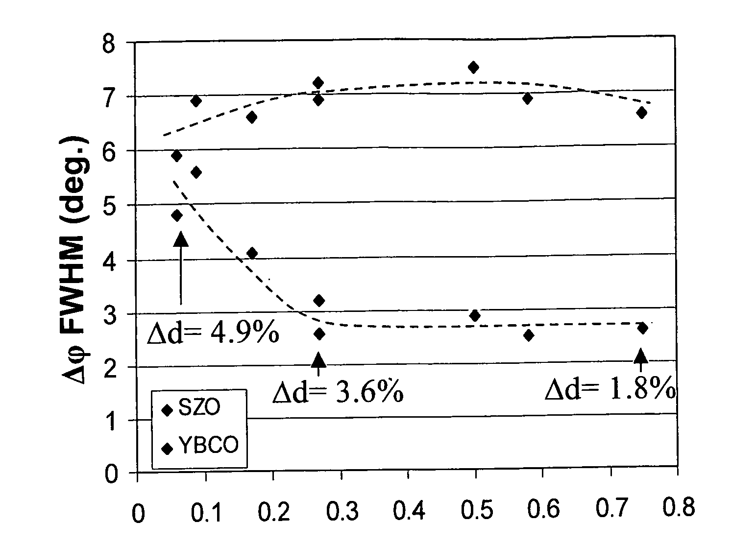
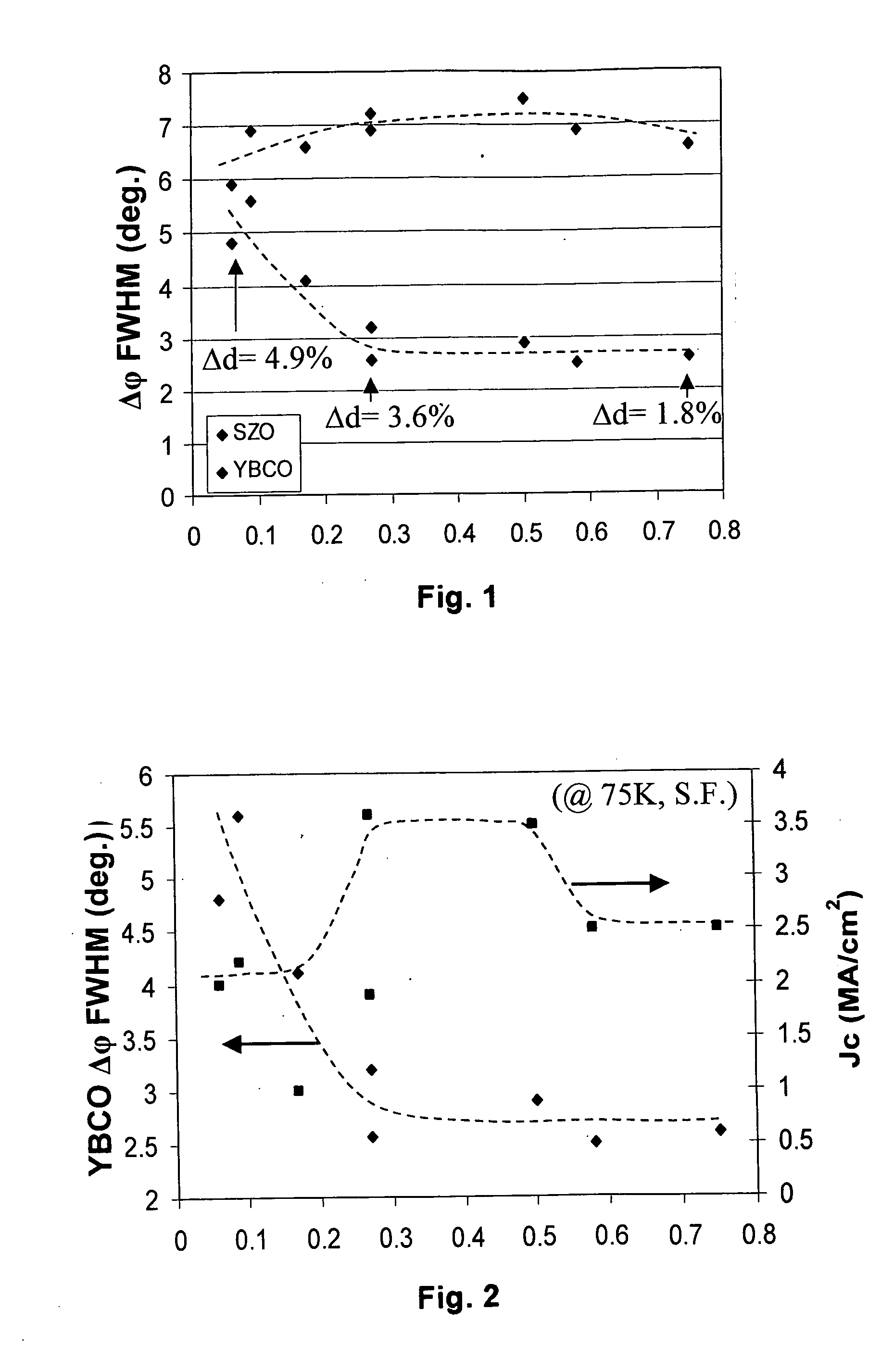
[0031] A coated conductor in accordance with the present invention was formed with the following structure: a Hastelloy base substrate / a layer of Al2O3 / a layer of Y2O3 / a layer of IBAD-MgO / a layer of BaZrO3 / a layer of SrTiO3 / a layer of YBCO. The layer of BaZrO3 was deposited by pulsed laser deposition using a substrate temperature of 820° C., a background oxygen pressure of 0.3 Torr until a barium zirconate thickness of about 20 nanometers was formed. A layer of strontium titanate was formed upon the barium zirconate layer by PLD. A YBCO layer was deposited onto the strontium titanate layer and from this structure, the measured properties of the YBCO layer (1.3 μm in thickness) were: a superconducting transition temperature (Tc) of 88 K, an in-plane texture of 2.4° full width half maximum (FWHM), an out-of-plane texture of 1.2° FWHM and a critical current density (Jc) of 3.0 megamperes per square centimeter (MA / cm2) at 75 K. The results for Jc are as high as current state of the art ...

example 2

[0032] A coated conductor in accordance with the present invention was formed with the following structure: a Hastelloy base substrate / a layer of Al2O3 / a layer of Y2O3 / a layer of IBAD-MgO / a layer of BaZrO3 / a layer of YBCO. The layer of BaZrO3 was deposited by pulsed laser deposition using a substrate temperature of 820° C., a background oxygen pressure of 0.3 Torr until a barium zirconate thickness of from about 50 to about 80 nanometers was formed. The YBCO layer was deposited directly upon the barium zirconate layer and from this structure, the measured properties of the YBCO layer (1.2 μm in thickness) were: a Tc of 87.7 K, an in-plane texture of 5° FWHM, an out-of-plane texture of 1.1° and a Jc of 1.5 MA / cm2. The results demonstrate that a barium zirconate layer can be used directly between the IBAD MgO layer and the YBCO and provide good barrier protection (in place of the homoepitaxial MgO and SrTiO3 layers) and performance.

example 3

[0033] A coated conductor in accordance with the present invention was formed with the following structure: a Hastelloy base substrate / a layer of Al2O3 / a layer of Y2O3 / a layer of IBAD-MgO / a layer of samarium zirconate (Sm0.2Zr0.8O1.7) / a layer of YBCO. The layer of Sm0.2Zr0.8O1.7 (about 30 nm in thickness) was deposited by reactive sputtering from metal targets of samarium and zirconium. The conditions used for the deposition included a substrate temperature of 750° C. and a background oxygen pressure of 1.0×10⁻² Torr. The texture for the samarium zirconate film was measured as about 5.9° FWHM for the in-plane texture and 2.8° FWHM for the out-of-plane texture. These texture values were very near those of the starting IBAD MgO template. After the deposition of the YBCO, the final YBCO in-plane texture value was 5° and 0.9° FWHM for the out-of-plane texture. The measured Tc was 92.0 K and the Jc was 0.9 MA / cm2 for a 1.2 micrometer thick YBCO film. These results demonstrate that a sama...


PUM

PropertyMeasurementUnit
thicknessaaaaaaaaaa
thicknessaaaaaaaaaa
superconducting transition temperatureaaaaaaaaaa

Abstract

Articles are provided including a base substrate having a layer of an IBAD oriented material thereon, and, a layer of barium-containing material selected from the group consisting of barium zirconate, barium hafnate, barium titanate, barium strontium titanate, barium dysprosium zirconate, barium neodymium zirconate and barium samarium zirconate, or a cubic metal oxide material selected from the group consisting of rare earth zirconates and rare earth hafnates upon the layer of an IBAD oriented material. Such articles can further include thin films of high temperature superconductive oxides such as YBCO upon the layer of barium-containing material selected from the group consisting of barium zirconate, barium hafnate, barium titanate, barium strontium titanate, barium dysprosium zirconate, barium neodymium zirconate and barium samarium zirconate, or a cubic metal oxide material selected from the group consisting of rare earth zirconates and rare earth hafnates.

Description

RELATED APPLICATIONS [0001] This application claims the benefit of provisional application Ser. No. 60 / 699,241 filed Jul. 13, 2005.STATEMENT REGARDING FEDERAL RIGHTS [0002] This invention was made with government support under Contract No. DE-AC52-06NA25396 awarded by the U.S. Department of Energy. The government has certain rights in the invention.FIELD OF THE INVENTION [0003] The present invention relates to high temperature superconducting thick films on substrates, e.g., polycrystalline substrates, such superconducting thick films having high Jc's and Ic's, and relates to structural template articles for subsequent deposition of an oriented film, e.g., of superconducting thick films. BACKGROUND OF THE INVENTION [0004] U.S. Pat. No. 6,756,139 described a coated conductor architecture based on ion beam assisted deposited magnesium oxide (IBAD-MgO), which comprises four or five separately deposited layers between the metal substrate and the superconducting layer. Among the describe...

Claims


Application Information

Patent Timeline
Patent Type & Authority Applications(United States)
IPC IPC(8): H01L29/94
CPCH01L39/2461H10N60/0632
Inventor ARENDT, PAULFOLTYN, STEPHENSTAN, LILIANAUSOV, IGORWANG, HAIYAN
Owner TRIAD NAT SECURITY LLC
Why Eureka
Try Eureka