Semiconductor device and method for producing the same

a semiconductor and semiconductor technology, applied in semiconductor devices, semiconductor/solid-state device details, electrical apparatus, etc., can solve the problems of lowering the withstand voltage of the device, complicated production process, and distorted equipotential lines, and achieve excellent withstand voltage performance, high reliability, and high withstand voltage configuration

Active Publication Date: 2007-01-18
MITSUBISHI ELECTRIC CORP
View PDF4 Cites 31 Cited by
  • Summary
  • Abstract
  • Description
  • Claims
  • Application Information

AI Technical Summary

Benefits of technology

[0025] With the present invention, a highly reliable semiconductor device having a high-withstand voltage configuration and being excellent in withstand voltage performance can be produced using a simple pro

Problems solved by technology

Hence, the elongation of a depletion layer that is formed on the N−-type epitaxial layer 3 is hindered, whereby there is a problem of lowering the withstand voltage of the device.
In the conventional semiconductor device, when the voltage required for the HVIC becomes high, there is a problem that equipotential lines are distorted owing to the fact that the GND-side field plate (the aluminum electrode 10) is not provided under the level shift wire and owing to the influence of the potential of the level shift wire, whereby field concentration occu

Method used


Image

  • Semiconductor device and method for producing the same
  • Semiconductor device and method for producing the same
  • Semiconductor device and method for producing the same

Examples


embodiment 1

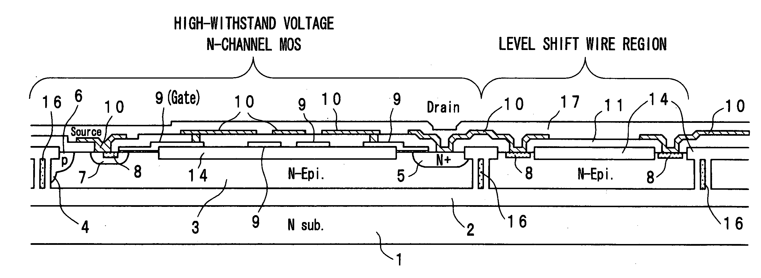
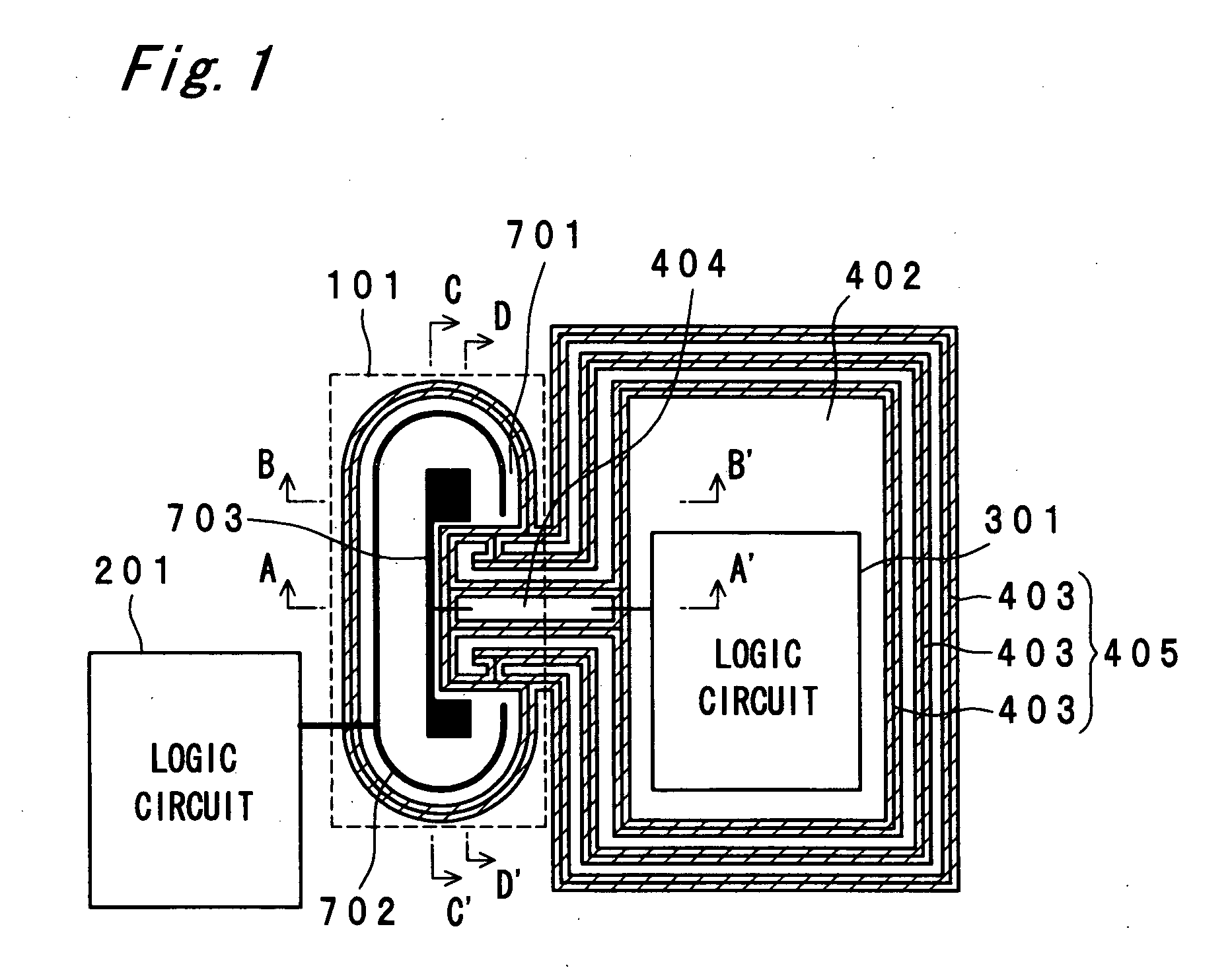
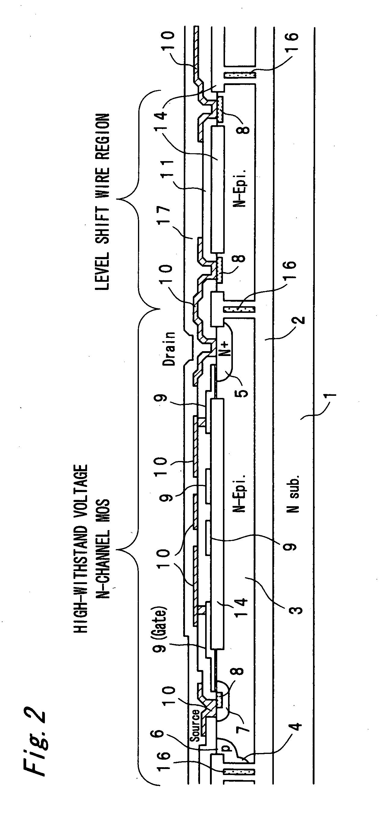
[0076]FIG. 1 is a plan view showing a power integrated circuit device (hereafter simply referred to as an HVIC) serving as an example of a semiconductor device according to Embodiment 1 of the present invention. In FIG. 1, this HVIC is schematically shown to facilitate the explanation of the HVIC according to Embodiment 1, and the sizes of its components and the spaces between them are different from those of an actual device. FIGS. 2 to 5 are sectional views of the HVIC shown in FIG. 1. FIG. 2 is a sectional view taken on line A-A′ of FIG. 1, FIG. 3 is a sectional view taken on line B-B′ of FIG. 1, FIG. 4 is a sectional view taken on line C-C′ of FIG. 1, and FIG. 5 is a sectional view taken on line D-D′ of FIG. 1.

[0077] As shown in FIG. 1, the HVIC according to Embodiment 1 comprises a high-withstand voltage N-channel MOSFET 101, a low-potential-side logic circuit 201 that is connected to the gate electrode 702 of the MOSFET 101 and outputs control signals for controlling the driv...

embodiment 2

[0102] A semiconductor device according to Embodiment 2 of the present invention will be described below referring to the accompanying drawings. FIG. 16 is a plan view showing a power integrated circuit device (HVIC) serving as the semiconductor device according to Embodiment 2. FIG. 16 schematically shows the HVIC to facilitate its explanation, and the sizes of its components and the spaces between them are different from those of an actual device. The HVIC according to Embodiment 2 has a configuration in which two or more high-withstand voltage N-channel MOSFETs 101 each having the level shift wire region 404 of the HVIC according to Embodiment 1 described above are arranged. FIG. 16 shows a configuration in which two high-withstand voltage N-channel MOSFETs 101 are arranged. In the HVIC according to Embodiment 2, the epitaxial regions and the polysilicon regions between the trench separation regions, divided using the level shift wire regions 404 are connected using aluminum wire...

embodiment 3

[0105] A semiconductor device according to Embodiment 3. of the present invention will be described below referring to the accompanying drawings. FIG. 17 is a plan view showing a power integrated circuit device (HVIC) serving as the semiconductor device according to Embodiment 3. FIG. 17 schematically shows the HVIC to facilitate its explanation, and the sizes of its components and the spaces between them are different from those of an actual device. FIG. 18 is a sectional view of the HVIC, taken on line A-A′ of FIG. 17.

[0106] In the HVIC according to the aforementioned Embodiment 1, the high-potential island 402 is separated using the multi-trench separation region 405, and the central trench in the level shift wire region 404 of the multi-trench separation region 405 is used as a level shift wire. In the case of this configuration, the resistance of the N -type epitaxial layer 3 is inserted as a wiring resistance, thereby constituting a restriction on the circuit configuration.

[...


PUM


Abstract

A semiconductor device is configured that a high-withstand voltage semiconductor device (101) and logic circuits (201 and 301) are integrated on a single chip and that a high-withstand voltage high-potential island (402) including the high-potential-side logic circuit (301) is separated using multiple partition walls enclosing therearound. The semiconductor device is provided with a multi-trench separation region (405) having a level shift wire region (404) that is used to connect the high-potential-side logic circuit to the high-potential-side electrode of the high-withstand voltage semiconductor device.

Description

FIELD OF THE INVENTION [0001] The present invention relates to a semiconductor device, more particularly, to a high-withstand voltage semiconductor device and a method for producing the same. BACKGROUND OF THE INVENTION [0002] As a conventional high-withstand voltage semiconductor device, a power integrated circuit device (HVIC: High Voltage IC) in which a power semiconductor device and logic circuits are integrated on a single chip has been used to control the driving of various apparatuses, such as motors, lighting apparatuses and imaging apparatuses. [0003]FIG. 44 is a plan view showing a conventional power integrated circuit device (hereafter simply referred to as an HVIC). FIGS. 45 to 48 are sectional views of the conventional HVIC shown in FIG. 44. FIG. 45 is a sectional view taken on line A-A′ of FIG. 44, FIG. 46 is a sectional view taken on line B-B′ of FIG. 44, and FIG. 47 is a sectional view taken on line C-C′ of FIG. 44. FIG. 48 is a block diagram showing the configuratio...

Claims


Application Information

Patent Timeline
IPC IPC(8): H01L23/58H01L21/8238
CPCH01L21/84H01L27/0922H01L27/1203H01L29/404H01L29/42368H01L29/7824H01L2924/0002H01L29/7835H01L29/8611H01L2924/00H01L21/76224H01L21/76281
Inventor SHIMIZU, KAZUHIRO
Owner MITSUBISHI ELECTRIC CORP
Why Eureka
Try Eureka