Organic and inorganic light active devices and methods for making the same

Inactive Publication Date: 2007-01-18
DANIELS JOHN J
View PDF10 Cites 52 Cited by
  • Summary
  • Abstract
  • Description
  • Claims
  • Application Information

AI Technical Summary

Benefits of technology

[0028] It is an object of the present invention to overcome the drawbacks of the prior art. It is an object of the present invention to provide a method of fabricating a light active device by dispersing three dimensionally a semiconductor particulate within a carrier material. The resulting structure has individual point sources of light emission dispersed within a protective barrier material. The barrier material provides strength to the device and adhesion to the electrodes and/or other films and prevents contamination of the semiconductor particulate. The inventive fabrication method also allows multiple colors to be emit

Problems solved by technology

Further, the absorption of light by the semiconductive polymer results in positive and negative charges that produce an electric current.
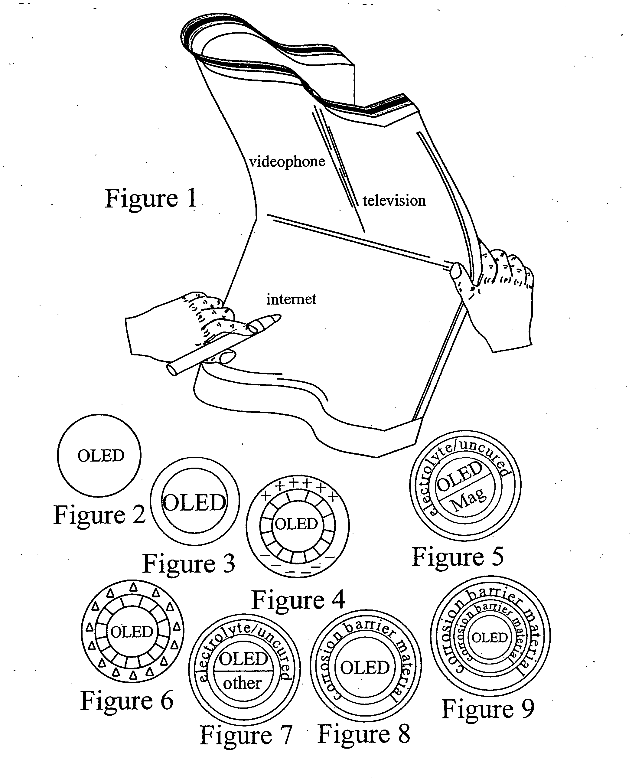
The unstoppable march of technology often changes the way we see the world.
One of the biggest challenges to the OLED display industry is from contamination by water and oxygen.
The materials involved in small molecule and polymer OLEDs are vulnerable to contamination by oxygen and water vapor, which can trigger early failure.
This issue is exacerbated when non-glass substrates are used.
Neither of these solutions is adequate, adding to the cost and complexity of forming an OLED device.
In the end, the problems caused by the ingress of water and oxygen to the organic stack continue to pose serious technical issues. FIG. 111 illustrates a prior art OLED device.
Such thin layers of organic material are susceptible to major problems, such as loss of film integrity, particularly when applied to a flexible substrate. FIG. 112 illustrates a prior art OLED device wherein a dust spec creates an electrical short between the electrodes.
The extreme thinness of the layers of organic material between conductors also results in electrical shorts easily forming due to even very small specks of dust or other contaminants.
Because of this limitation, costly cleanroom facilities must be built and maintained using the conventional OLED thin film fabrication techniques.
However, there are some serious disadvantages to the adapting of inkjet printing to OLED display fabrication.
Inkjet printing does not adequately overcome the problem of material degradation by oxygen and water vapor. FIG. 113 illustrates a prior art OLED device wherein the thin organic film stack is degraded by the ingress of oxygen and/or water.
Elaborate and expensive materials and fabrication processes are still required to provide adequate encapsulation to protect and preserve the thin organic films.
It is difficult to align display pixel-sized electrodes and inkjet printed OLED material with the accuracy needed to effect a high resolution display.
However, there are still some technical hurdles that remain to be solved before OLED displays will realize their commercial potential.
One of the biggest challenges to the OLED display industry is from contamination by water and oxygen.
The materials involved in small molecule and polymer OLEDs are vulnerable to co

Method used


Image

  • Organic and inorganic light active devices and methods for making the same
  • Organic and inorganic light active devices and methods for making the same
  • Organic and inorganic light active devices and methods for making the same

Examples


Example

[0250] For purposes of promoting an understanding of the principles of the invention, reference will now be made to the embodiments illustrated in the drawings and specific language will be used to describe the same. It will nevertheless be understood that no limitation of the scope of the invention is thereby intended, there being contemplated such alterations and modifications of the illustrated device, and such further applications of the principles of the invention as disclosed herein, as would normally occur to one skilled in the art to which the invention pertains.

[0251]FIG. 1 illustrates an embodiment of the inventive thin, lightweight, flexible, bright wireless display having components capable of being manufactured by the inventive display fabrication method, showing the simultaneous display of mapped hyperlinked content, a videophone stream and a broadcast TV stream. FIG. 1 illustrates an embodiment of an inventive thin, lightweight, flexible, bright, wireless display sho...


PUM

PropertyMeasurementUnit
Concentrationaaaaaaaaaa
Electric potential / voltageaaaaaaaaaa
Lightaaaaaaaaaa

Abstract

A light active device includes a semiconductor particulate dispersed within a carrier material. A first contact layer is provided so on application of an electric field charge carriers having a polarity are injected into the semiconductor particulate through the carrier material. A second contact layer is provided so on application of the electric field to the second contact layer charge carriers having an opposite polarity are injected into the semiconductor particulate through the carrier material. The semiconductor particulate comprises at least one of an organic and an inorganic semiconductor. The semiconductor particulate may comprise an organic light active particulate. When constructed as a light emitting device, an electric field applied to the semiconductor particulate through the carrier causes charge carriers of opposite polarity to be injected into the semiconductor particulate. The charge carriers combine to form carrier pairs which decay and give off light.

Description

CROSS-REFERENCE TO RELATED APPLICATIONS [0001] This is a divisional application of U.S. Ser. No. 10 / 716,794, filed Nov. 19, 2003, which is a utility application of provisional application Ser. No. 60 / 469,667, filed May 12, 2003, and is a continuation-in-part of U.S. Utility patent application Ser. No. 10 / 375,161, filed Feb. 26, 2003, which is a continuation-in-part of U.S. Utility patent application Ser. No. 10 / 321,161, filed Dec. 17, 2002 which is the U.S. Utility patent application of a Provisional Patent Application Ser. No. 60 / 427,333, filed Nov. 19, 2002. This application is related to co-pending patent application Ser. No. 10 / 234,302 filed Sep. 4, 2002 and U.S. patent application Ser. No. 10 / 234,301 filed Sep. 4, 2002, the subject matter of these patent documents is incorporated by reference herein in its entirety.BACKGROUND OF THE INVENTION [0002] The present invention pertains to organic and inorganic light active devices, and hybrids thereof, and methods of making the same....

Claims


Application Information

Patent Timeline
IPC IPC(8): B05D5/12H05B33/20
CPCB82Y20/00H05B33/20C09K11/06C09K2211/14H01L27/3209H01L27/3281H01L51/0008H01L51/5012H01L51/5048H01L51/52H01L51/5278H01L51/5287H01L2251/5369H05B33/10B82Y30/00H10K59/32H10K59/17H10K71/16H10K50/14H10K50/80H10K50/19H10K50/182H10K50/11H10K2102/331
Inventor DANIELS, JOHN JAMES
Owner DANIELS JOHN J
Why Eureka
Try Eureka