Supercharge Your Innovation With Domain-Expert AI Agents!

Process for growing silicon single crystal and process for producing silicon wafer

a technology of silicon single crystal and growing process, which is applied in the direction of crystal growth process polycrystalline material growth, etc., can solve the problems of large cavity consisting of hydrogen defects, deterioration of gate oxide integrity, etc., and achieve the effect of increasing the pulling rate margin of a defect-free crystal, reducing the number of parts, and reducing the number of defects

Active Publication Date: 2007-01-25
SUMCO CORP
View PDF5 Cites 12 Cited by
  • Summary
  • Abstract
  • Description
  • Claims
  • Application Information

AI Technical Summary

Benefits of technology

[0030] The inventors of the present invention have thoroughly researched and found that, as described later, it is possible to suppress the generation of hydrogen defects by using an atmospheric gas for growing a single crystal which is a hydrogen-containing gas which contains a hydrogen-containing substance having a concentration ranging from 40 to 400 Pa in terms of a hydrogen gas reduced partial pressure, and pulling the silicon single crystal at a pulling rate ranging from a value with which the ratio (a / b) of the diameter (b) of the silicon single crystal and the outer diameter (a) of a ring which consists of an OSF-generating region in the radial direction of the silicon single crystal is not higher than 0.77 to another value with which said OSF-generating region disappears at the center part of the crystal.
[0073] As the process for forming an epitaxial layer, a method which is performed generally can be used, thereby it is possible to obtain an epitaxial silicon wafer with no COP (laser scattering tomography defect) trace, even if it is a thin epitaxial layer having a thickness of not more than approximately 0.5 to 2 μm.

Problems solved by technology

However, as integrated circuits have been down-sized in recent years, deterioration of gate oxide integrity due to a laser scattering tomography defect has been pointed out.
In the technology disclosed in Patent document 1, it is possible to suppress the generation of COP, which is a laser scattering tomography defect, by adding hydrogen into the pulling furnace, without decreasing the pulling rate to be not higher than the critical pulling rate at which an OSF-generating region will be generated, however, in the case of growing a silicon single crystal at a pulling rate which is not lower than the critical pulling rate at which an OSF-generating region will be generated, a large cavity consisting of a hydrogen defect will be generated, which has been a problem.
The hydrogen defect will not disappear even if it is subjected to a heat treatment, and hence it is impossible to use a silicon single crystal in which hydrogen defects exist as a silicon wafer for use in a semiconductor.

Method used


Image

  • Process for growing silicon single crystal and process for producing silicon wafer
  • Process for growing silicon single crystal and process for producing silicon wafer
  • Process for growing silicon single crystal and process for producing silicon wafer

Examples


experimental examples 6 to 12

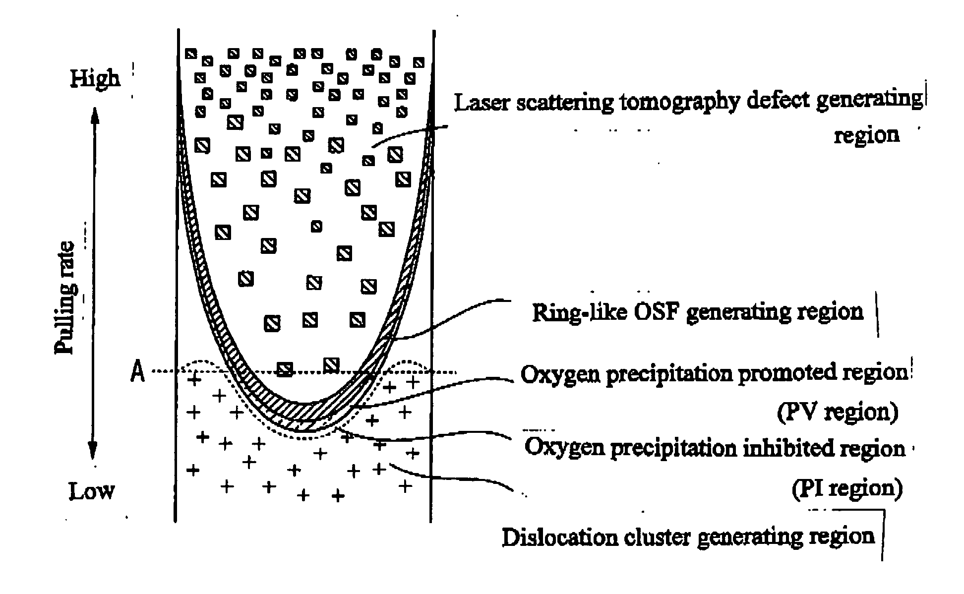
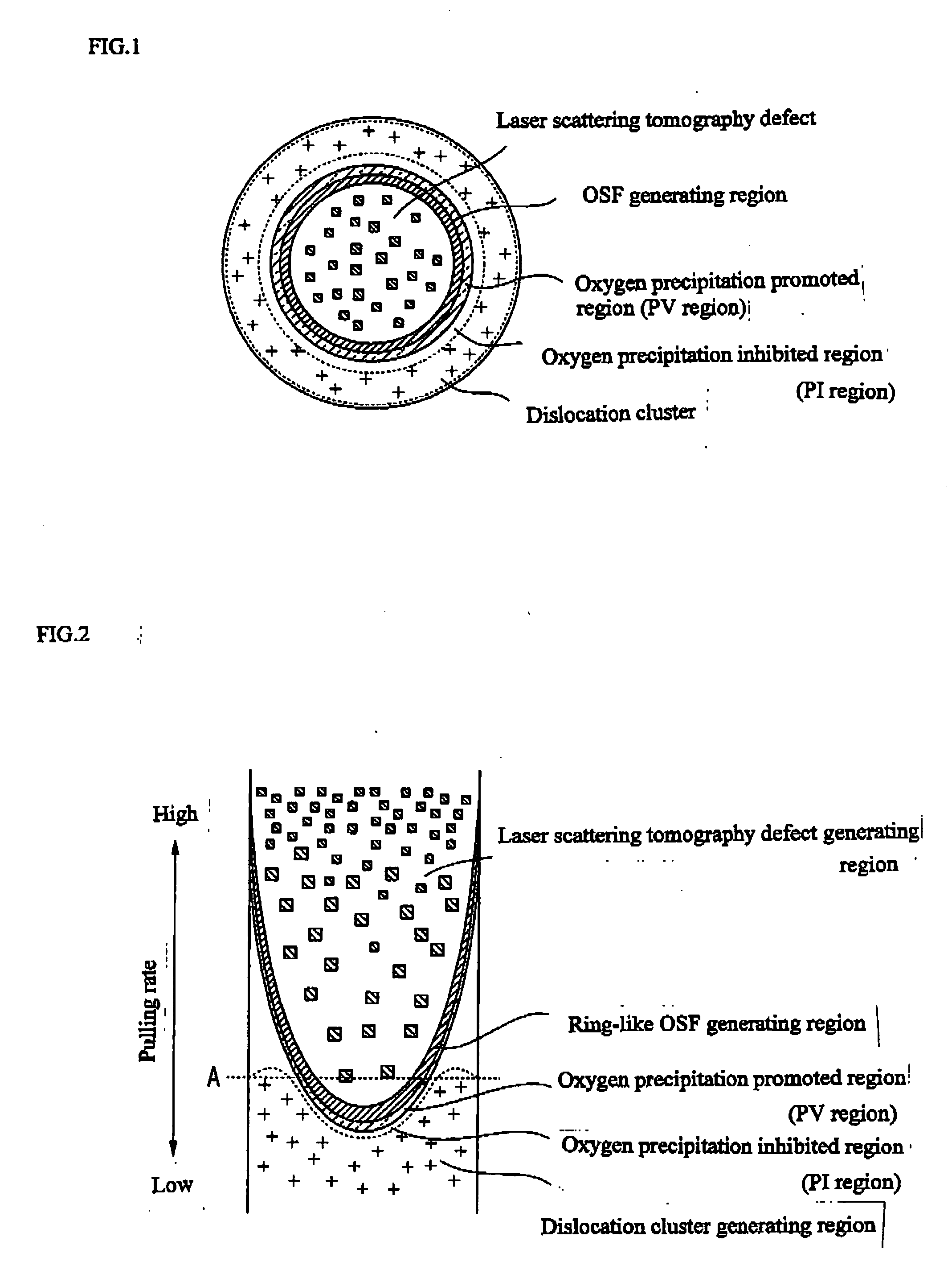
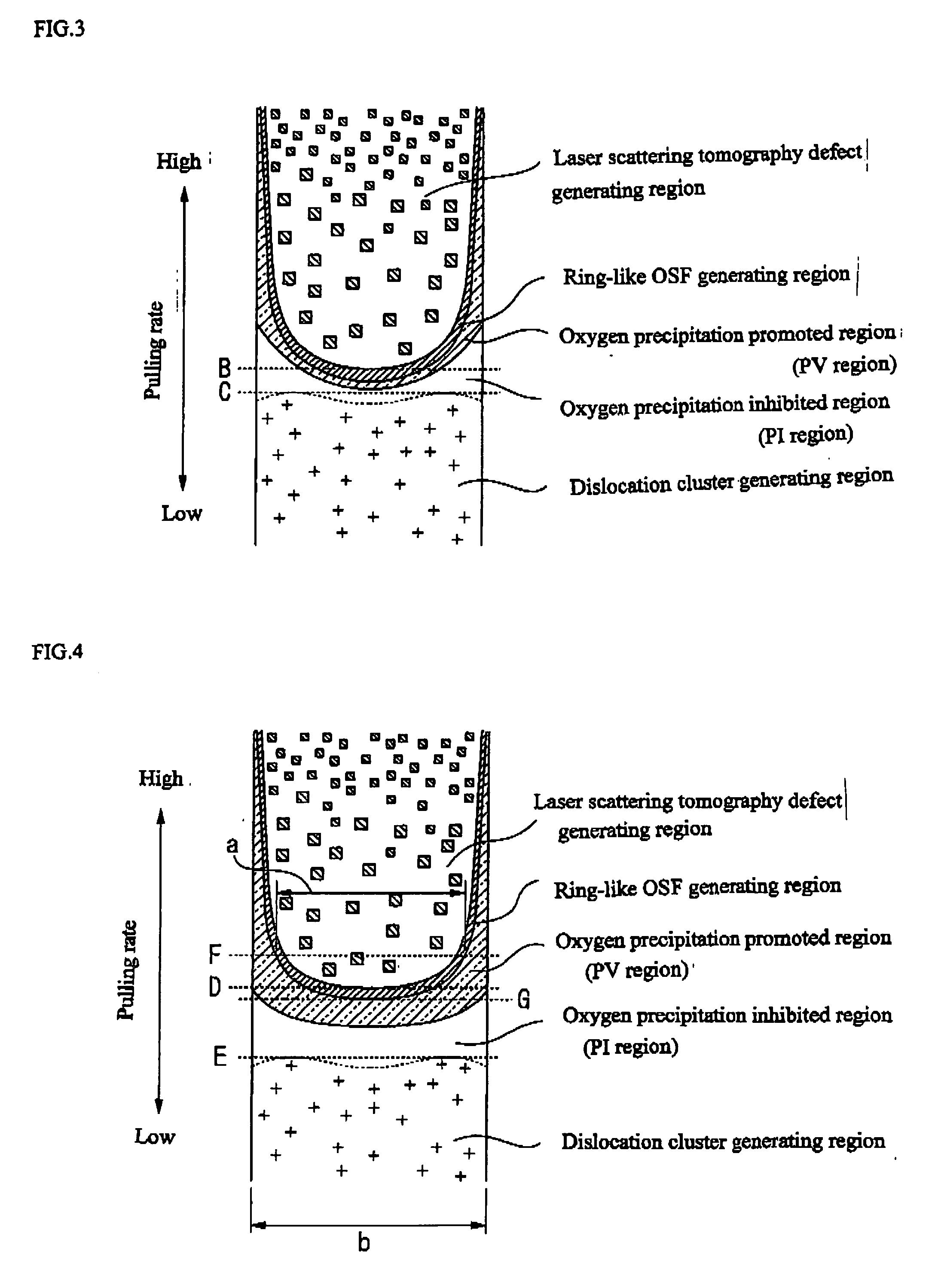
[0119] A silicon single crystal with a diameter of 300 mm was grown at a higher pulling rate than that at which the OSF region disappears at the crystal central part, using an apparatus for growing a silicon single crystal having a hot-zone structure in which the temperature gradient (Gc) in the crystal central part was the same as or greater than (Gc≧Ge) the temperature gradient (Ge) in a crystal perimeter part, while supplying an inert gas to which hydrogen was added to the pulling furnace so as to obtain the hydrogen molecular partial pressure in Experimental Examples 6 to 12 shown in Table 2, and then the resultant silicon single crystal was sliced to obtain a silicon wafer.

TABLE 2Position whereH2 PartialOSF-ring existsNumber ofPresence orExperimentalpressure(Wafer diameterLPDabsence of Example(Pa)ratio) (a / b)(pieces / wf)H2 defect6No doping0.48113. . .7300.5187None8400.7312None9400.262None102400.684Present112400.8843None124000.533None

[0120] With respect to the silicon wafer of ...

experimental examples 13 to 19

[0130] A silicon single crystal with a diameter of 300 mm was grown at a higher pulling rate than that at which the OSF region disappeared at the crystal central part, using the same apparatus for growing a silicon single crystal as in Experimental Examples 6 to 12, while supplying an inert gas to which hydrogen was added to the pulling furnace so as to obtain the hydrogen molecular partial pressure in Experimental Examples 13 to 19 shown in Table 3, and then the resultant silicon single crystal was sliced to obtain a silicon wafer.

TABLE 3Position wherethe OSF-ringH2 Partialexists (WaferNumber of Epi-defect (piece / wf)ExperimentalpressurediameterEpi-thicknessEpi-thicknessEpi-thicknessEpi-thicknessExample(Pa)ratio) (a / b)0.3 μm0.5 μm2 μm4 μm13No0.48694358624doping14300.5134316145315400.73587114316400.27141214172400.69645831182400.901145291817194000.55493722

Note:

“Epi” in Table 3 means “Epitaxial Layer”

[0131] With respect to the silicon wafer of Experimental Examples 13 to 19 thus obt...

experimental examples 20 to 26

[0139] A silicon single crystal with a diameter of 300 mm was grown at a higher pulling rate than that at which the OSF region disappeared at the crystal central part, using the same apparatus for growing a silicon single crystal as in Experimental Examples 6 to 12, while supplying an inert gas to which hydrogen was added to the pulling furnace so as to obtain the hydrogen molecular partial pressure in Experimental Examples 20 to 26 shown in Table 4, and then the resultant silicon single crystal was sliced to obtain a silicon wafer.

TABLE 4PositionNumber ofNumber ofwhere theCOP afterCOP afterH2 PartialOSF-ring existsgrindinggrindingExperimentalpressure(Wafer diameterby 5 μmby 10 μmExample(Pa)ratio) (a / b)(pieces / wf)(pieces / wf)20No doping0.49432721300.55313422400.776223400.2993242400.6578252400.872121264000.5956

[0140] With respect to the silicon wafer of Experimental Examples 20 to 26 thus obtained, the ratio (a / b) of the outer diameter (a) in the radial direction of the silicon sing...


PUM

PropertyMeasurementUnit
diameteraaaaaaaaaa
diameteraaaaaaaaaa
sizeaaaaaaaaaa

Abstract

A process for growing a silicon single crystal which is capable of growing a silicon single crystal at a pulling rate which is not lower than the critical pulling rate at which an OSF-generating region will be generated is provided. Such a process for growing a silicon single crystal is characterized by using an atmospheric gas for growing a single crystal which is a hydrogen-containing gas which contains a hydrogen-containing substance, and pulling the silicon single crystal at a pulling rate ranging from a value with which the ratio (a / b) of the diameter (b) of the silicon single crystal and the outer diameter (a) of a ring which consists of the OSF-generating region in the radial direction of the silicon single crystal is not higher than 0.77 to another value with which the OSF-generating region disappears at the center part of the crystal.

Description

BACKGROUND OF THE INVENTION [0001] 1. Field of the Invention [0002] The present invention relates to a process for growing silicon single crystal and a process for producing a silicon wafer, in particularly, to a process for growing silicon single crystal which is capable of pulling it up at a pulling rate at which a silicon single crystal including a laser scattering tomography defect-generating region is grown, without generating a hydrogen defect. [0003] Priority is claimed on Japanese Patent Application No. 20005-208525, filed Jul. 19, 2005, the content of which is incorporated herein by reference. [0004] 2. Description of the Related Art [0005] As a production method for a silicon single crystal which is a material of a silicon wafer, a growing method by the Czochralski method (referred to as “CZ method” hereinafter) is known. [0006] It is known that minute defects will be formed during the production process of a device, i.e. a grown-in defect is generated in the silicon singl...

Claims


Application Information

Patent Timeline
Patent Type & Authority Applications(United States)
IPC IPC(8): C30B15/00C30B21/06C30B27/02C30B28/10C30B30/04
CPCC30B29/06C30B15/203
Inventor ONO, TOSHIAKISUGIMURA, WATARUHOURAI, MASATAKA
Owner SUMCO CORP
Features
  • R&D
  • Intellectual Property
  • Life Sciences
  • Materials
  • Tech Scout
  • Unparalleled Data Quality
  • Higher Quality Content
  • 60% Fewer Hallucinations
Learn More