Semiconductor memory device

a memory device and semiconductor technology, applied in the field of semiconductor memory devices, can solve the problems of enlargement of the layout area of the memory mat, increase in the number of sense amplifiers and write amplifiers, etc., and achieve the effect of reducing reducing the parasitic capacitance connected to the first common data line, and minimizing the increase in the number of write amplifiers

Active Publication Date: 2007-01-25
RENESAS ELECTRONICS CORP
View PDF2 Cites 11 Cited by
  • Summary
  • Abstract
  • Description
  • Claims
  • Application Information

AI Technical Summary

Benefits of technology

[0005] In a DRAM, one sense amplifier is provided for a pair of bit lines. However, when one sense amplifier is disposed for a pair of bit lines in an SRAM, the layout area increases. Consequently, it is usually constructed so that a pair of common read data lines and a pair of common write data lines are connected to a plurality of bit lines, the number of sense amplifiers and the number of write amplifiers are the same, and the number of common read data line pairs and the number of common write data line pairs are the same. In such a configuration, to increase the speed of reading operation on a memory cell in which read current is small, it is considered to decrease the number of bit line pairs associated with a pair of common read data lines. However, decrease in the number of bit line pairs associated with a pair of common data lines in an SRAM means increase in the number of sense amplifiers and write amplifiers, and it causes enlargement of the layout area of a memory mat.
[0006] An object of the present invention is to provide a technique for increasing the reading speed while suppressing enlargement of the layout area of a memory mat.
[0010] By setting the number of bit lines corresponding to the second common data line to be smaller than the number of bit lines corresponding to the first common data line, while minimizing increase in the number of write amplifiers, parasitic capacitance connected to the first common data line can be reduced. Thus, time in which the potential difference between the pair of common read data lines can be shortened, so that increase in the speed of reading can be achieved while suppressing enlargement of the layout area of a memory mat.
[0012] In short, increase in the speed of reading can be achieved while suppressing enlargement of the layout area of a memory mat.

Problems solved by technology

However, decrease in the number of bit line pairs associated with a pair of common data lines in an SRAM means increase in the number of sense amplifiers and write amplifiers, and it causes enlargement of the layout area of a memory mat.

Method used


Image

  • Semiconductor memory device
  • Semiconductor memory device
  • Semiconductor memory device

Examples


Embodiment Construction

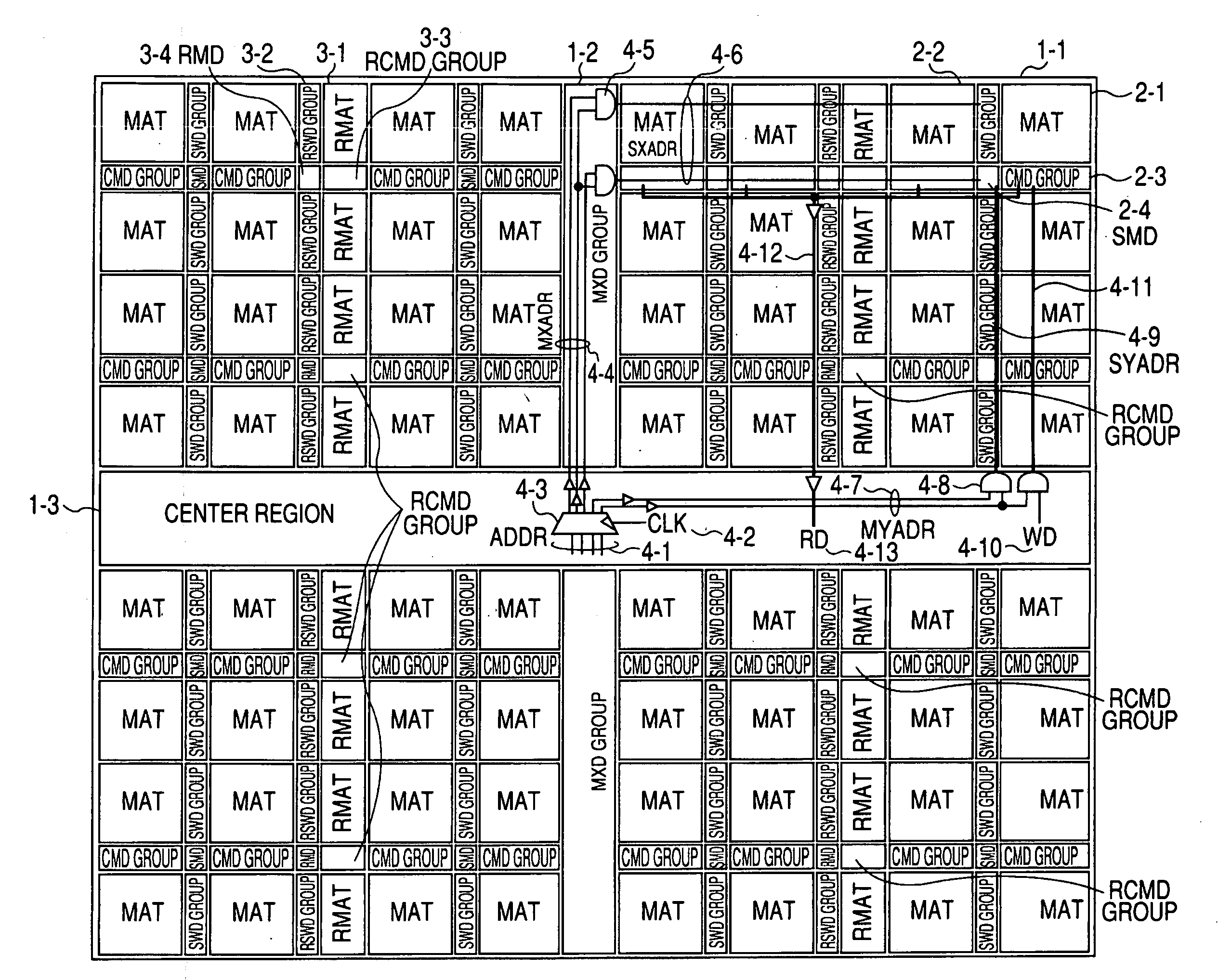
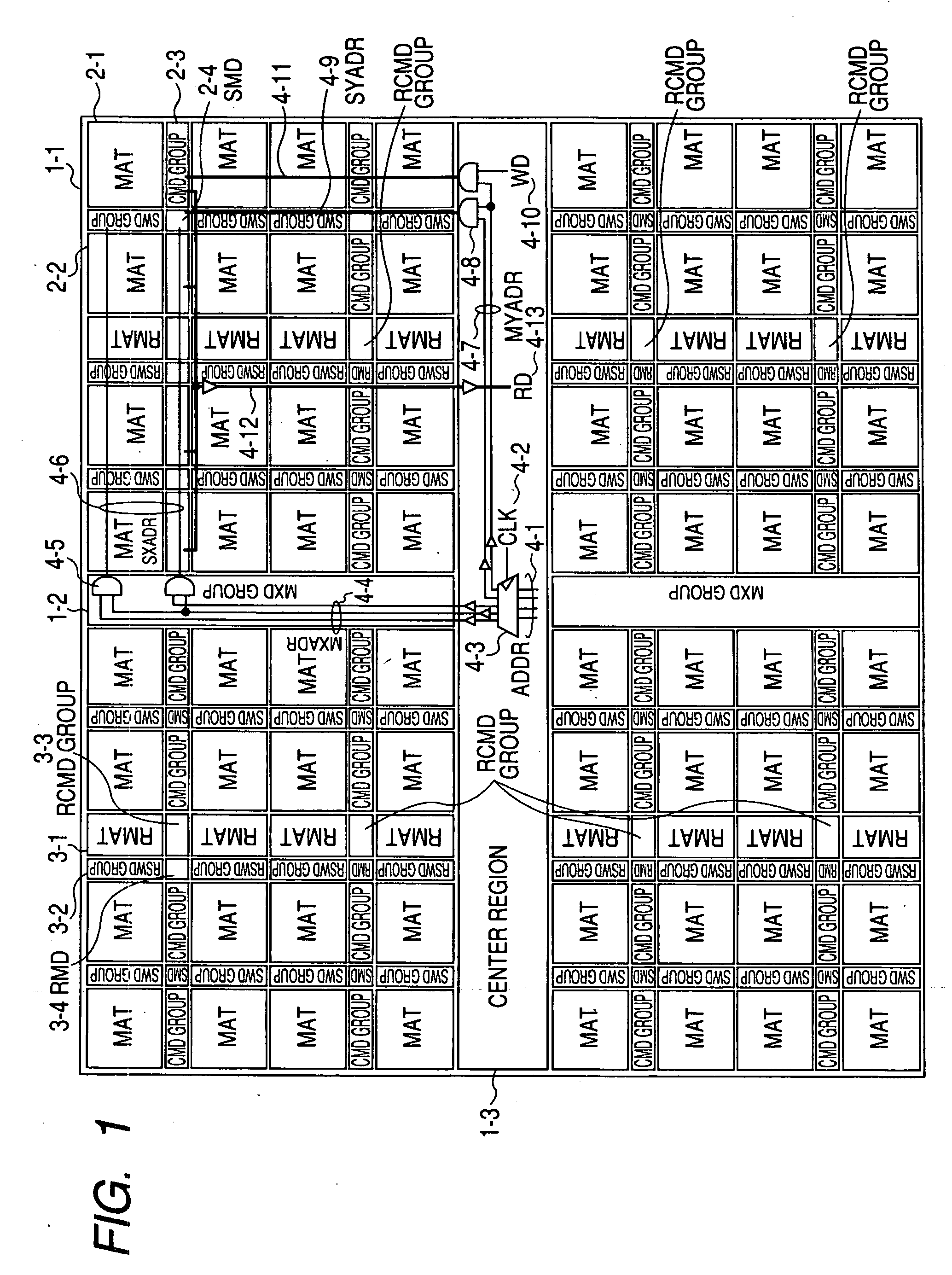
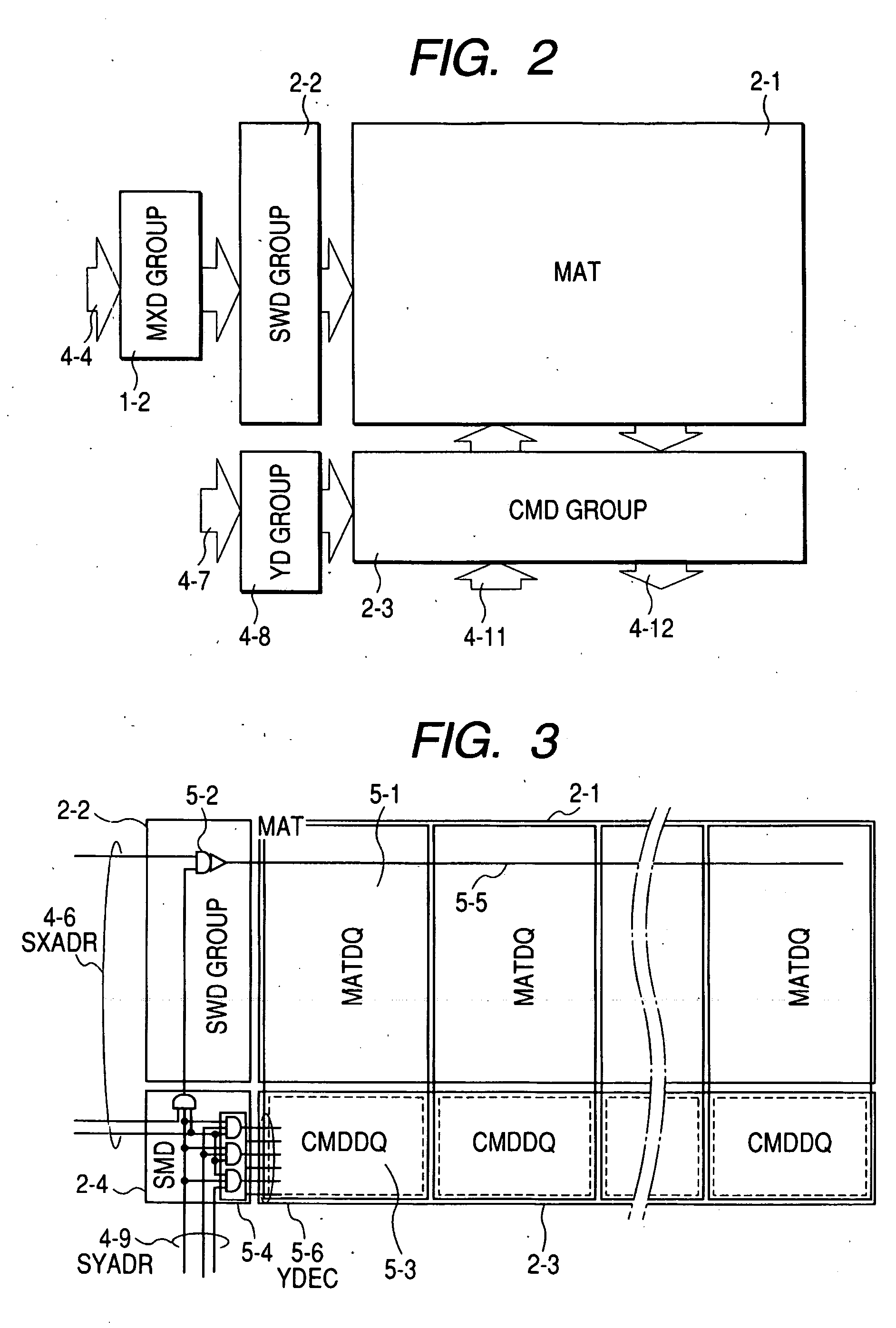
[0035]FIG. 1 shows an SRAM as an example of a semiconductor memory device according to the present invention. FIG. 2 schematically shows the relation between one of a plurality of memory mats in the SRAM illustrated in FIG. 1 and peripheral circuits of the memory mat.

[0036] An SRAM 1-1 shown in FIG. 1 is, although not limited, formed on a semiconductor substrate such as a single crystal silicon substrate by a known semiconductor integrated circuit manufacturing technique.

[0037] The SRAM 1-1 is divided into four areas by a center region 1-3 and a main X decode circuit group (MXD group) 1-2 formed so as to cross the center region 1-3. In each of the four areas, a plurality of normal memory mats (MAT) 2-1, a plurality of normal sub word driver groups (SWD groups) 2-2, a plurality of normal column selection circuit groups (CMD groups) 2-3, a plurality of sub mat decode circuits (SMD) 2-4, a plurality of redundancy memory mats (RMAT) 3-1, a plurality of redundancy sub word driver group...


PUM


Abstract

The present invention provides a semiconductor memory device in which the number of write amplifiers is decreased by increasing the number of bit line pairs connected to one pair of common write data lines. Further, by decreasing the number of bit line pairs connected to one pair of common read data lines, parasitic capacitance connected to the pair of common read data lines is reduced and, accordingly, time in which the potential difference between the pair of common read data lines increases is shortened. Thus, while preventing enlargement of the chip layout area, read time can be shortened.

Description

CROSS-REFERENCE TO RELATED APPLICATION [0001] The present application claims priority from Japanese patent application No. 2005-211182 filed on Jul. 21, 2005, the content of which is hereby incorporated by reference into this application. BACKGROUND OF THE INVENTION [0002] The present invention relates to a semiconductor memory device and, more particularly, to a technique for improving layout of the semiconductor memory device. The invention relates to, for example, a technique which is effectively applied to a static memory in which static memory cells are connected to a plurality of word lines and a plurality of bit lines disposed so as to cross the word lines. [0003] Examples of the semiconductor memory device include a dynamic random access memory (abbreviated as “DRAM”) using dynamic memory cells as memory cells as disclosed in Japanese Unexamined Patent Publication No. 2001-344965 (Patent Document 1) and a static random access memory (abbreviated as “SRAM”) using static memor...

Claims


Application Information

Patent Timeline
Patent Type & Authority Applications(United States)
IPC IPC(8): G11C5/06
CPCG11C7/02G11C7/1051G11C7/106G11C7/1069G11C11/4097G11C7/1084G11C7/18G11C11/4087G11C11/4093G11C7/1078
Inventor SATO, HAJIMESHINOZAKI, MASAO
Owner RENESAS ELECTRONICS CORP
Why Eureka
Try Eureka