

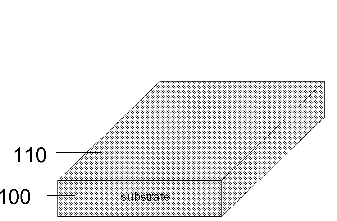
Flexible Structures For Sensors And Electronics
a technology of flexible structures and electronics, applied in the direction of sustainable manufacturing/processing, instruments, ornamental textile articles, etc., can solve the problems of significant limitations in electronic performance, limited flexibility of flexible electronic devices, and limitations of conventional polymer-based substrates relevant to the development of high-performance flexible electronic devices, etc., to achieve the effect of avoiding damage or significant degradation of device performan
- Summary
- Abstract
- Description
- Claims
- Application Information
AI Technical Summary
Benefits of technology
Problems solved by technology
Method used
Image

Examples
example 1
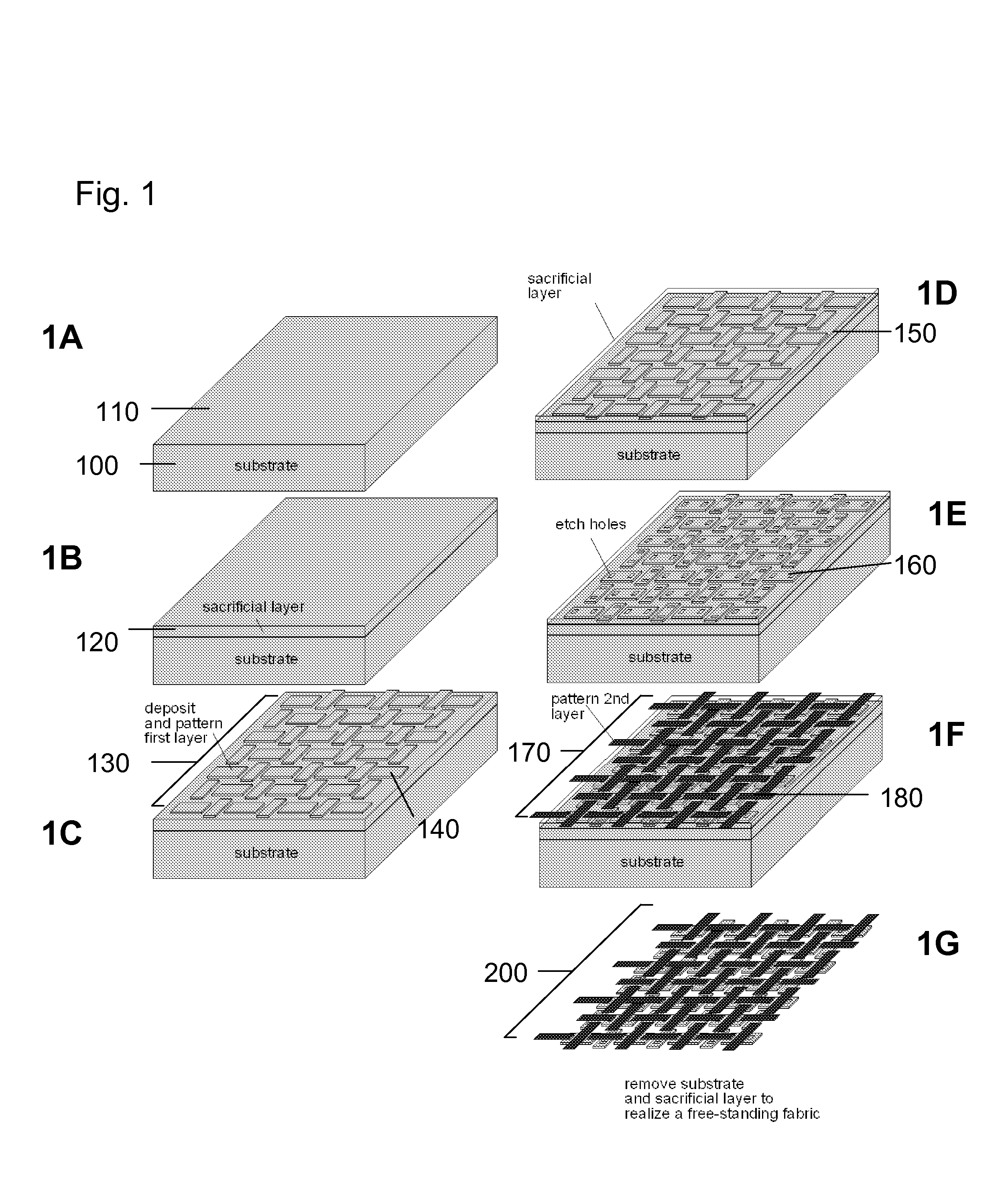
Fabrication of a Metallic Micro-Machined Fabric
[0069] The ability of the present invention to provide a flexible, metallic micro-machined fiber was verified by experimental studies. Specifically, it is a goal of the present invention to provide methods of making flexible, metallic micro-machined fiber capable of conforming to contoured surfaces having a large radius of curvature with significant damage or degradation. Further, it is a goal of the present invention to provide methods of making flexible, metallic micro-machined fiber capable of significantly stretching and bending without fracture.
[0070] To verify these capabilities of the methods and free-standing structures of the present invention, a metallic micromachined fabric was fabricated and tested with respect to important mechanical properties. The fabric, similar in construction to chain mail, consists of small rings and links built upon a planar substrate and then released to yield a flexible and mechanically robust sh...
example 2
Fabrication of a Parylene Micro-Machined Fabric
[0079] The ability of the present invention to provide flexible, polymer-based micro-machined fibers was verified by experimental studies. Specifically, a micromachined fiber comprising a woven network of parylene elements was fabricated using the present methods and examined with respect to its mechanical properties.
[0080]FIG. 11 shows a process flow diagram useful for fabricating a micromachined fiber comprising a woven network of interconnected parylene elements. As shown in FIG. 11, an aluminum sacrificial layer is deposited onto a substrate. A first parylene structural layer is next deposited onto the aluminum sacrificial layer, and is covered with an aluminum patterning layer. The exposed aluminum patterning layer is patterned by selectively removing material and the patterned aluminum layer and first parylene structural layer are subjected to etching, thereby patterning the first parylene structural layer. Referring again to FI...
example 3
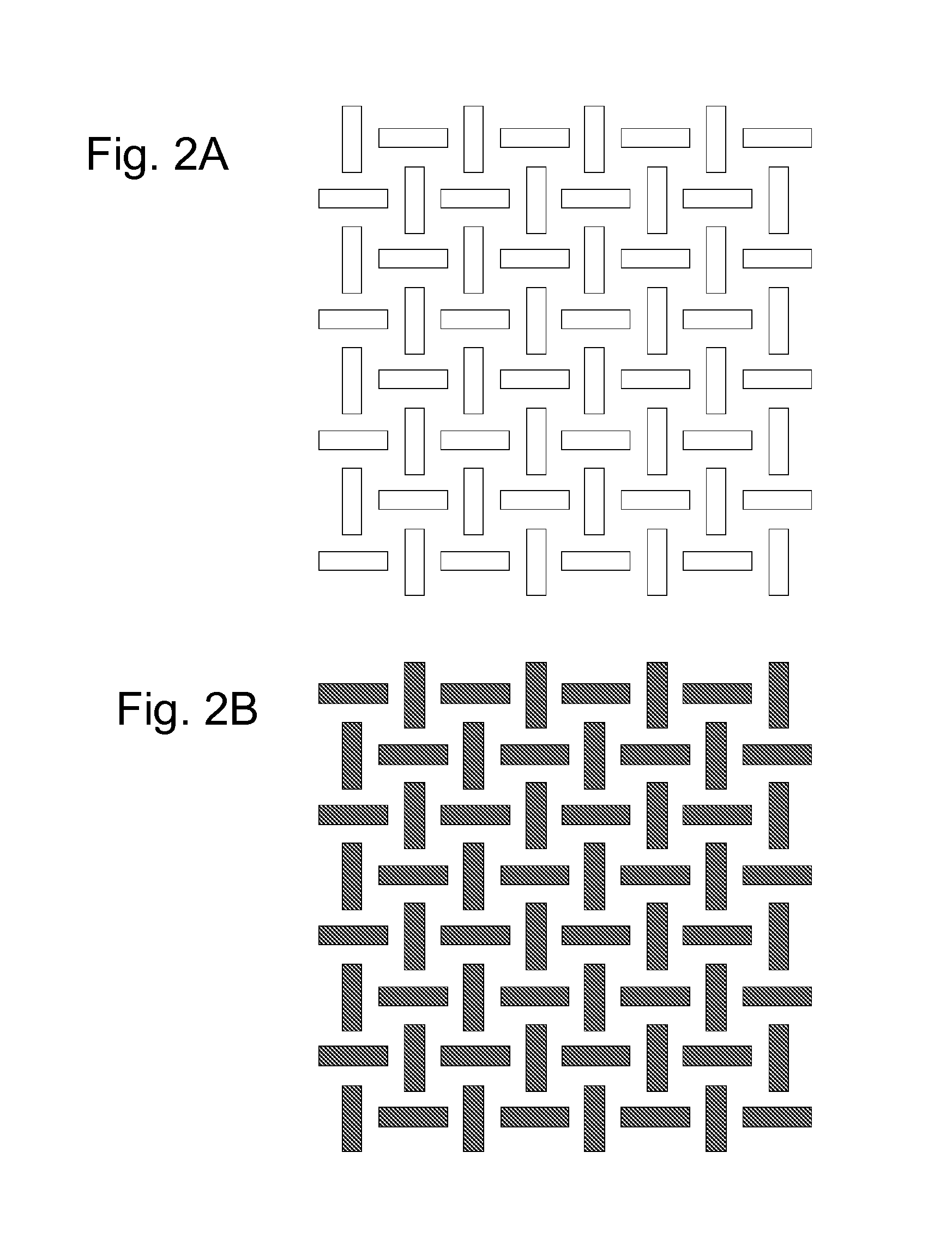
Flexible Skin with Two-Axis Bending Capability Made Using Weaving-by-Lithography Fabrication Method
[0083] In this Example, we demonstrate the general design of a two-axis bendable flexible skin of the present invention and its companion fabrication method. Conventional flexible skins typically are only bendable along one axis. For example, they may be rolled onto circular cylinder conformally but not onto sphere. The flexible skin of the present example features a novel interwoven structure. The horizontal and vertical threads of the skin are not connected; they are free to slide and rotate against each other, therefore enabling the skin to adjust its shape to conform to complex curvatures. To demonstrate the functional benefits of this aspect of the present invention, we have embedded passive RF elements (planar coil inductors) inside the skin. The inductance value is experimentally determined to be 106 μH.
3.a. Introduction
[0084] Conventional flexible skins can achieve good con...
PUM
| Property | Measurement | Unit |
|---|---|---|
| thicknesses | aaaaa | aaaaa |
| surface area | aaaaa | aaaaa |
| temperatures | aaaaa | aaaaa |
Abstract
Description
Claims
Application Information