Method for forming film pattern, and method for manufacturing device, electro-optical device, electronic apparatus and active matrix substrate

a technology of film pattern and manufacturing method, which is applied in the direction of double resist layer, photomechanical equipment, instruments, etc., can solve the problems of difficult stably forming fine patterns, large equipment requirements for photolithography, and high manufacturing costs, so as to achieve uniform thickness, rapid and reliable supply, and the effect of stably providing

Inactive Publication Date: 2007-01-25
SEIKO EPSON CORP
View PDF16 Cites 13 Cited by
  • Summary
  • Abstract
  • Description
  • Claims
  • Application Information

AI Technical Summary

Benefits of technology

[0011] An advantage of the invention is to provide a method for forming a film pattern that can uniformly and stably form a film pattern by providing a functional liquid to a pattern forming region that includes regions having a different width.
[0012] A method for forming a film pattern according to a first aspect of the invention includes: disposing a first bank forming material to a substrate so as to form a first bank layer; disposing a second bank forming material on the first bank layer so as to form a second bank layer; and pattering the first bank layer and the second bank layer so as to form a bank including a pattern forming region having a first pattern forming region and a second pattern forming region. The second pattern forming region has a width larger than a width of the first pattern forming region, and is continuously formed from the first pattern forming region. The first bank layer has a sidewall facing the pattern forming region and a first contact angle of less than 50 degrees on the sidewall with respect to a functional liquid containing H2O. The second bank layer has a second contact angle larger than the first contact angle with respect to the functional liquid.
[0013] According to the method, the functional liquid disposed in the pattern forming region can wet and spread with a specific shape since the first bank layer, which is disposed as a lower layer, has the first contact angle of less than 50 degrees with respect to the functional liquid on the sidewall of the first bank layer. Namely, the leading edge of the functional liquid that wets and spreads can have a concave shape, both parts of which extend in a spreading direction along the sidewalls of the pattern forming region in a plan view. This specific shape allows the functional liquid to spread uniformly and rapidly in the pattern...

Problems solved by technology

However, the photolithography needs large-scale equipment such as vacuum apparatuses and exposure apparatuses, and sophisticated processes to form the wiring line having a predetermined pattern.
In addition, almost all of materials are wasted due to a low efficiency of about several percent in using the materials, resulting in high manufacturing costs.
However, in the pattern forming method using the droplet discharge method described above, it is difficult to stably form a fine pattern since a discharged droplet spreads on a substrate after landing on the substrate.
Particularly, when the pattern functions as a conductive film, spreading of the droplet causes a liquid pool (bulge), which may cause a failure such as wire breakage or short.
As a result, a problem arises in that the film thickness of a formed fine wiring pattern is thinner than other wiring patterns.
How...

Method used


Image

  • Method for forming film pattern, and method for manufacturing device, electro-optical device, electronic apparatus and active matrix substrate
  • Method for forming film pattern, and method for manufacturing device, electro-optical device, electronic apparatus and active matrix substrate
  • Method for forming film pattern, and method for manufacturing device, electro-optical device, electronic apparatus and active matrix substrate

Examples


first embodiment

[0055] First Embodiment

[0056] An embodiment of the invention will be described with reference to the accompanying drawings. The embodiment described below is shown by way of example, and not intended to limit the invention. It should be noted that different scales are used for the layers and members in the drawings, so that the layers and members can be recognized.

[0057] Droplet Discharge Device

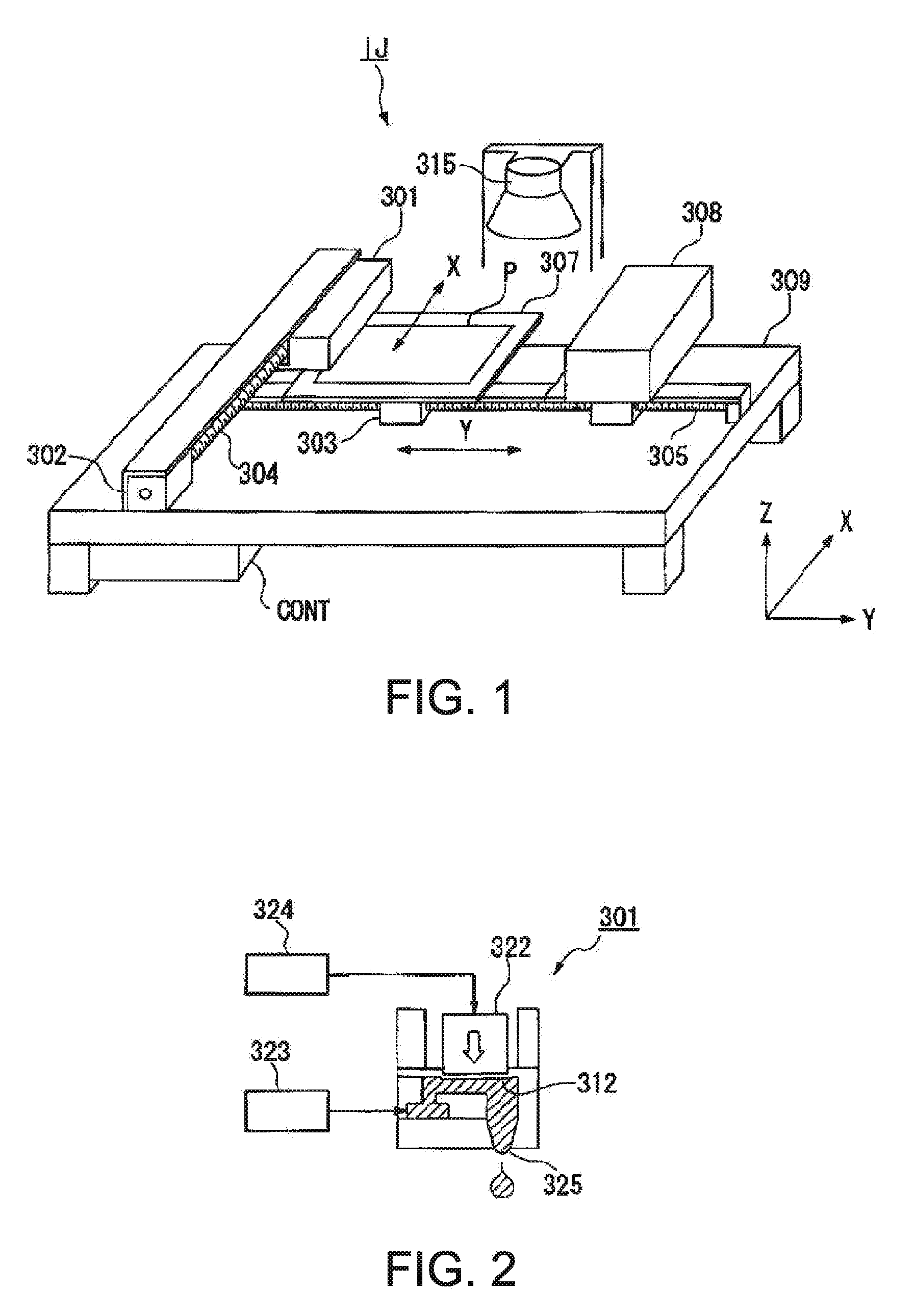
[0058] First, a droplet discharge device, which is used to form a film pattern in the embodiment, will be described with reference to FIG. 1.

[0059]FIG. 1 is a perspective view illustrating a schematic structure of a droplet discharge device (inkjet device) IJ that disposes a functional liquid on a substrate by a droplet discharge method as an example of devices used for the method for forming a film pattern according to the invention.

[0060] The droplet discharge device IJ includes a droplet discharge head 301, an X-axis direction drive axis 304, a Y-axis direction guide axis 305, a contro...

second embodiment

[0123] Second embodiment

[0124] In the first embodiment, a case is described in which a film pattern made of single material is formed. However, the method for forming a film pattern according to the invention is also favorable compared to related art when a film pattern is formed as a multilayerd structure of a plurality of materials. For example, a two-layer structure may be employed in a gate wiring line included in a pixel of an electro-optical device. The two-layer structure is composed of a base layer formed by using one or two or more metal materials chosen from Ag, Cu, Al, or the like, and a covering layer formed by using one or two or more metal materials chosen from Ni, Ti, W, Mn or the like. The two-layer structure prevents Ag, Cu, Al, or the like included in the base layer from diffusing into a gate insulation film with the covering layer, thereby a TFT is prevented from a malfunction, a low electron mobility, or the like. In addition, an adhesive layer (e.g. Mn is used) ...

third embodiment

[0127] Third Embodiment

[0128] Device

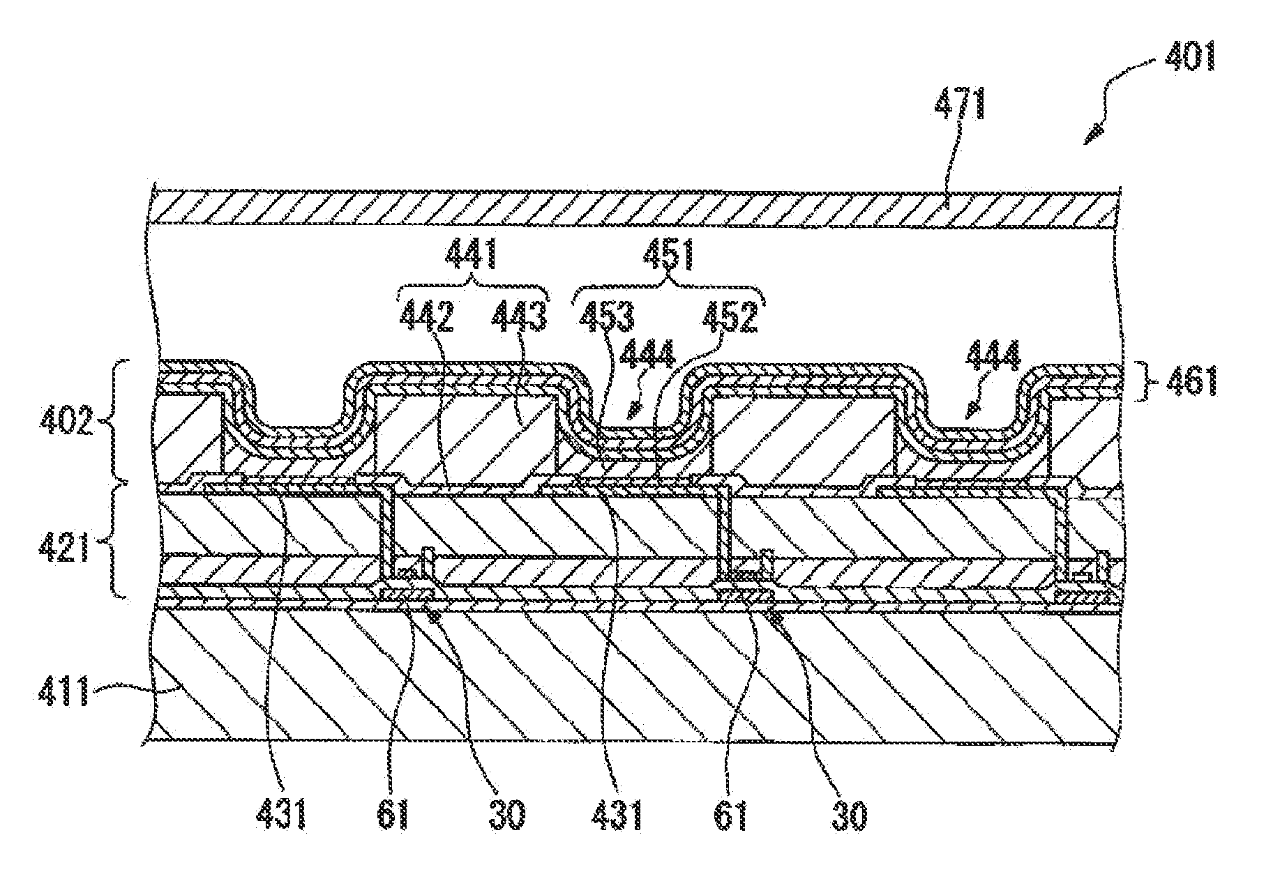
[0129] Next, a device will be described that has a film pattern formed by the method for forming a film pattern according to the invention. In a third embodiment, a pixel (device) having a gate wiring line, and a method for forming the pixel will be described with reference to FIGS. 7 and 8.

[0130] In the embodiment, a pixel, which includes a gate electrode, a source electrode, a drain electrode, and the like of a TFT 30 of a bottom gate type, is formed by using the above-described methods for forming a bank structure and a film pattern. In the following description, the description of the same process in the film pattern forming processes shown in FIGS. 5 and 6 will be omitted. The structural element the same as that in the first embodiment is given the same numeral.

[0131] Structure of a Pixel

[0132] First, the structure of a pixel (device) having a film pattern formed by the method for forming a film pattern will be described.

[0133]FIG. 7 sho...


PUM


Abstract

A method for forming a film pattern, comprises: disposing a first bank forming material to a substrate so as to form a first bank layer; disposing a second bank forming material on the first bank layer so as to form a second bank layer; and pattering the first bank layer and the second bank layer so as to form a bank including a pattern forming region having a first pattern forming region and a second pattern forming region, the second pattern forming region having a width larger than a width of the first pattern forming region, and being continuously formed from the first pattern forming region, wherein the first bank layer has a sidewall facing the pattern forming region and a first contact angle of less than 50 degrees with respect to a functional liquid containing H2O on the sidewall, and the second bank layer has a second contact angle larger than the first contact angle with respect to the functional liquid.

Description

BACKGROUND [0001] 1. Technical Field [0002] The present invention relates to a method for forming a film pattern, and a method for manufacturing a device, an electro-optical device, an electronic apparatus, and an active matrix substrate. [0003] 2. Related Art [0004] As a method for forming a wiring line, which has a predetermined pattern, and is used in electric circuits and integrated circuits, photolithography has been widely used. However, the photolithography needs large-scale equipment such as vacuum apparatuses and exposure apparatuses, and sophisticated processes to form the wiring line having a predetermined pattern. In addition, almost all of materials are wasted due to a low efficiency of about several percent in using the materials, resulting in high manufacturing costs. [0005] Alternatively, a method is proposed in which a wiring line having a predetermined pattern is formed on a substrate using a droplet discharge method (called an inkjet method) in which a liquid mate...

Claims


Application Information

Patent Timeline
IPC IPC(8): H01L21/8234
CPCH01L27/3295H01L29/66765H01L51/0005H05K3/125H01L27/1292H05K2201/09727H05K2203/013H05K2203/0568H05K2203/0577H05K3/1258H10K59/122H10K71/135G03F7/0002
Inventor HIRAI, TOSHIMITSUMORIYA, KATSUYUKI
Owner SEIKO EPSON CORP
Why Eureka
Try Eureka