Variable capacitor and manufacturing method thereof
a manufacturing method and variable capacitor technology, applied in variable capacitors, capacitors with electrode area variation, fixed capacitors, etc., can solve the problems of dielectric loss, inability to change the electrostatic capacity of the voltage, and the voltage variation of the voltage variation capacitor, so as to prevent the energy loss of the input signal, reduce the distance between the electrodes, and remove the kind of reflected signal
- Summary
- Abstract
- Description
- Claims
- Application Information
AI Technical Summary
Benefits of technology
Problems solved by technology
Method used
Image
Examples
first embodiment
(First Embodiment)
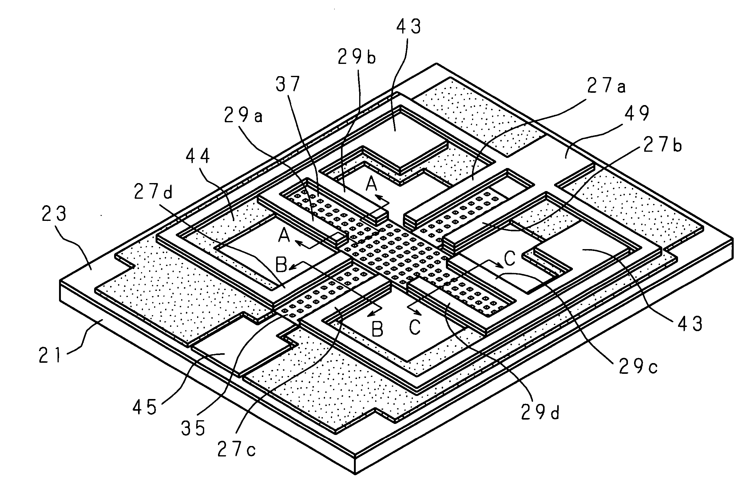
[0040]FIG. 3 is a pictorial view of the variable capacitor of a first embodiment of the present invention, and FIG. 4 is an exploded pictorial view of the same. In the figure, 21 is a substrate that is formed using a compound semiconductor. A cross-shaped opening 40 is formed in the center section of that substrate 21, and an insulating layer 23 is formed on the top surface of the substrate 21.
[0041] In the figure, 35 is a lower movable electrode and 37 is an upper movable electrode, where both are made of aluminum (Al). The lower movable electrode 35 comprises line sections 35a, 35a on both ends to form a first electrode section, and a central capacitor section 35b to form a second electrode section, where the end section of one of the line sections 35a is connected to a signal pad 45 to which a signal is inputted from an external high-frequency-signal source (not shown in the figure), and the end section of the other line section 35a is connected to the insulati...
second embodiment
(Second Embodiment)
[0057]FIG. 10 is an exploded pictorial view of the variable capacitor of a second embodiment of the invention, and FIG. 11 and FIG. 12 are cross-sectional drawings showing the manufacturing process for this variable capacitor.
[0058] In this second embodiment, there is a space 50 around the lower movable electrode 35, upper movable electrode 37, lower-movable-electrode actuator 27 and upper-movable-electrode actuator 29 between the lower movable electrode 35, upper movable electrode 37 and insulating layer 23 and the substrate 21. Also, instead of being made of silicon, the substrate 21 is formed from a material such as glass, sapphire, alumina, glass ceramic, gallium arsenic, or the like. The remaining construction is the same as that of the first embodiment, and the same reference numbers are given to identical sections.
[0059] After forming a second sacrificial layer 51 made from silicon using a sputtering method on top of the substrate 21 that is made from a m...
third embodiment
(Third Embodiment)
[0063]FIG. 13 is an exploded pictorial view of the variable capacitor of a third embodiment of the invention (only the movable electrode and actuator), and FIG. 14 and FIG. 15 are cross-sectional drawings showing the manufacturing process for this variable capacitor.
[0064] In this third embodiment, a dielectric layer 46 is located between the lower movable electrode 35 (capacitor section 35b) and the upper movable electrode 37 (capacitor section 37b). The other construction is the same as that of the first embodiment, and the same reference numbers are given to identical sections and an explanation is omitted.
[0065] This dielectric layer 46 can be located on the side of the upper movable electrode 37 (capacitor section 37b) as shown in FIG. 13, or on the side of the lower movable electrode 35 (capacitor section 35b) (not shown in the figure). The mass of the movable section is increased by using this dielectric layer 46, so the resonant frequency is slightly lowe...
PUM
 Abstract
Description
Claims
Application Information


