Substrate with light-shielding film, color filter substrate, method of manufacture of both, and display device having substrate with light-shielding film

a technology of light-shielding film and substrate, which is applied in the direction of photomechanical equipment, identification devices, instruments, etc., can solve the problems of occurrence of reverse taper shape, inability to obtain satisfactory etching profiles, and air accumulation

Inactive Publication Date: 2007-02-01
MITSUBISHI ELECTRIC CORP
View PDF6 Cites 16 Cited by
  • Summary
  • Abstract
  • Description
  • Claims
  • Application Information

AI Technical Summary

Benefits of technology

[0018] The above and other objects, features and advantages of the present invention will become more fully understood from the detailed description given hereinbelow and the accompanying drawings which are given by way of illustration only, and thus are not to be considered as limiting the present invention.

Problems solved by technology

As disclosed in Japanese Unexamined Patent Application Publication No. 11-194333, it is known that when etching a Cr / CrOx multilayer structure, there is the problem of occurrence of a reverse-taper shape.
Consequently the etching end face assumes a discontinuous shape, or assumes a reverse-taper shape or similar, and there is the problem that a satisfactory etching profile cannot be obtained.
Hence air accumulates in the portions of poor coverage of the color filter layer, air bubbles occur within the display panel, or lines are broken in the electrode film.
As a result, display defects may occur.
However, when using a method in which the flow rate of gas is controlled during film deposition and the degree of oxidation or the degree of nitrification is continuously changed, there have been the following problems.
However, there has been the problem that during the limited film deposition time, it is exceedingly difficult to continuously change the flow rate of the oxygen gas or nitrogen gas so as to uniformly change the mixture ratio.
In this case, there is unevenness in the distribution of the degree of oxidation or the degree of nitrification within the substrate plane.
As a result, etching cannot be performed satisfactorily.
In this case, the film thickness must be made extremely thin at each step, and so it becomes difficult to secure uniformity of film thickness.
Moreover, there is the further problem that the film deposition time becomes extremely long, so that productivity declines.
Hence for practical purposes it is difficult to use this method for film deposition.
When such etching profiles occur the coverage is reduced, and display quality is degraded.
However, even when the angle of the etching end face is made vertical, if the light-shielding film is thick the step is sharp, and coverage declines.
As a result, display defects have occurred.
In the above-described display devices of the related art, when a light-shielding film having a chromium oxide film is used, a satisfactory etching profile cannot be obtained, and there is the problem of display quality degradation resulting from reduced coverage.

Method used


Image

  • Substrate with light-shielding film, color filter substrate, method of manufacture of both, and display device having substrate with light-shielding film
  • Substrate with light-shielding film, color filter substrate, method of manufacture of both, and display device having substrate with light-shielding film
  • Substrate with light-shielding film, color filter substrate, method of manufacture of both, and display device having substrate with light-shielding film

Examples


first embodiment

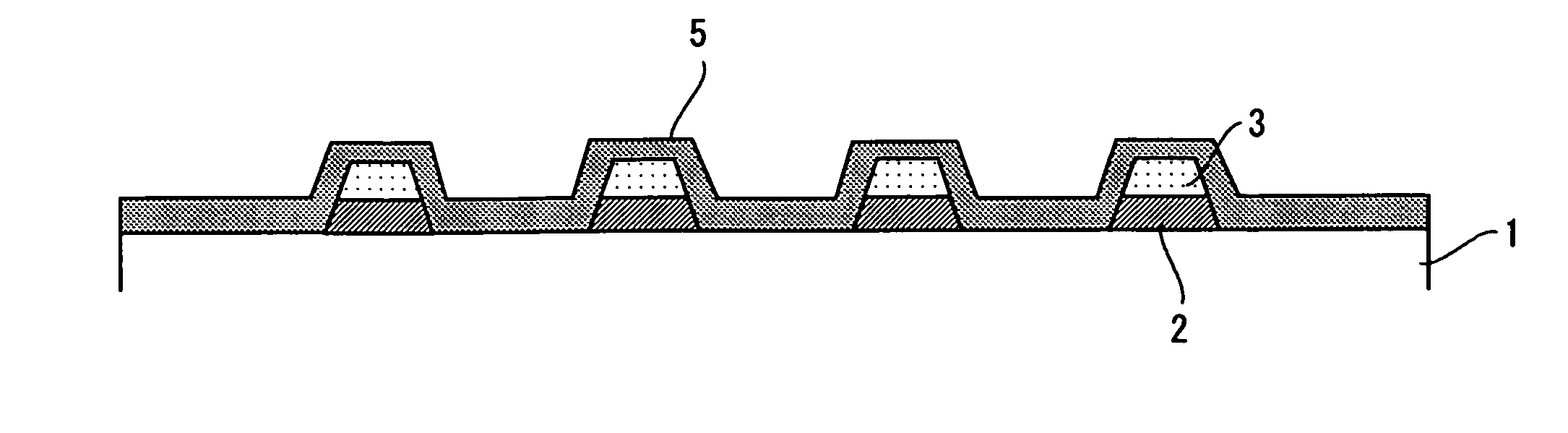
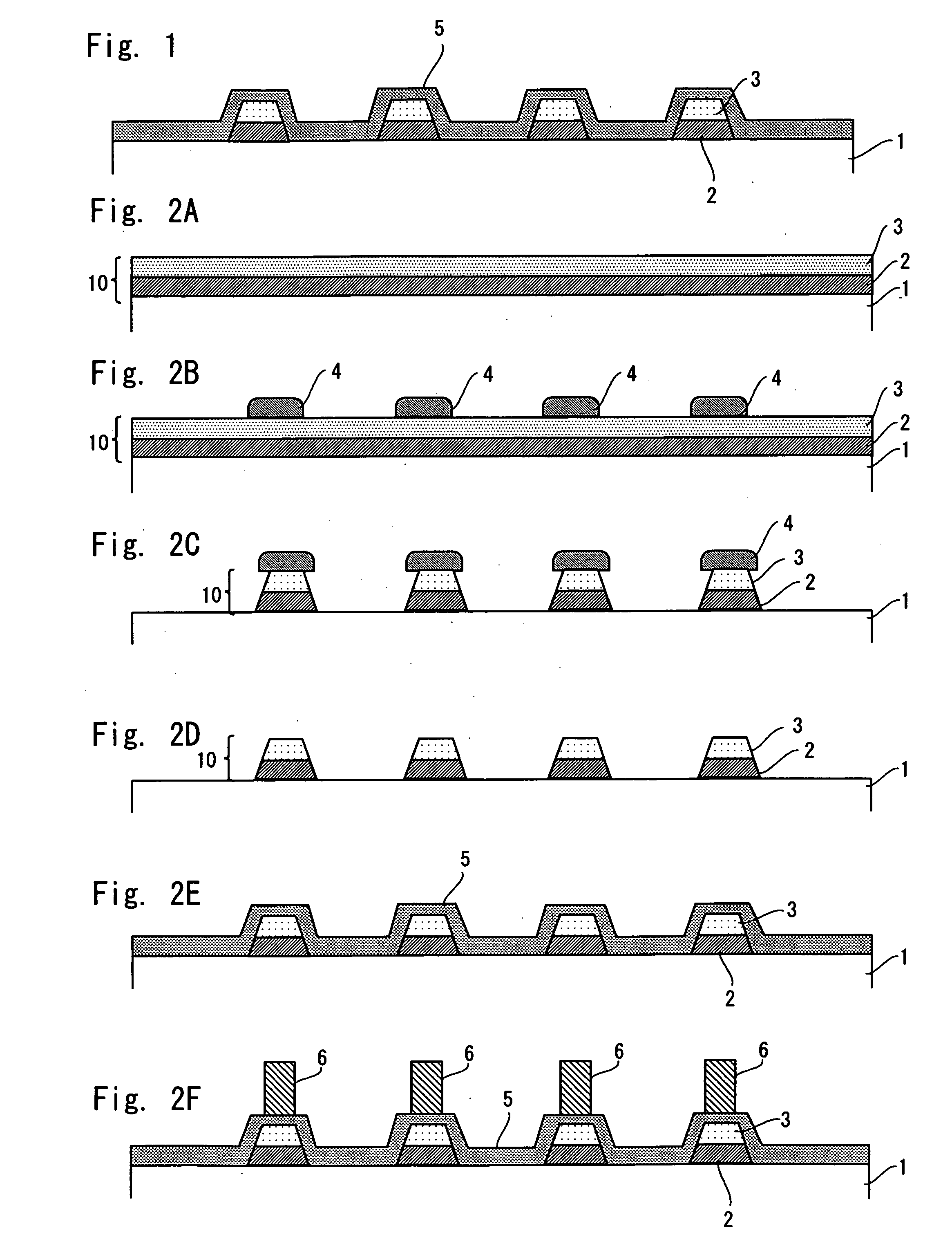
[0029] In this embodiment, a substrate with a light-shielding film is explained assuming use in a field-sequential type liquid crystal display device. In FIG. 1, 1 is the substrate, 2 is a first film, 3 is a second film, and 5 is a transparent conductive film.

[0030] The substrate 1 comprises, for example, glass or another transparent insulator. The first film 2 is formed on the substrate 1. The first film 2 comprises for example chromium oxide, having low reflectivity. That is, the first film 2 is formed from CrOx film (where x is a positive number) with low reflectivity. The degree of oxidation of the first film 2 is substantially constant. The second film 3 is formed on the first film 2. The second film 3 comprises for example metallic chromium, with high opacity. That is, the second film 3 is formed from Cr film with high opacity. The multilayer film comprising the first film 2 and second film 3 serves as the light-shielding film.

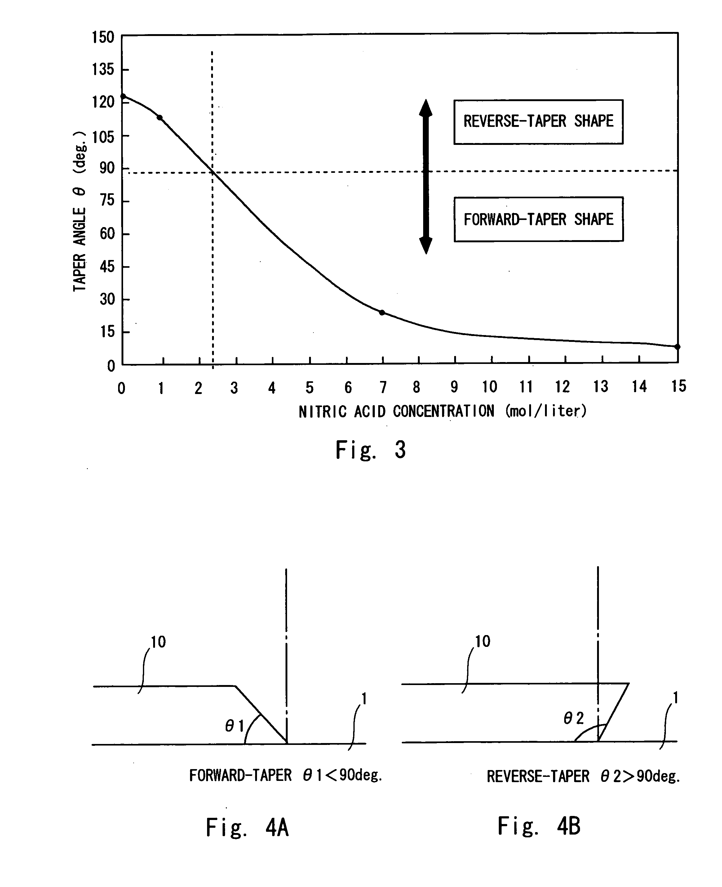
[0031] The light-shielding film is patterned to ...

second embodiment

[0053] The configuration of a substrate with a light-shielding film of this embodiment is explained using FIG. 7. FIG. 7 is a side cross-sectional view showing the configuration of the substrate with a light-shielding film. In this embodiment, an example of application of this invention to a color filter substrate, which is an opposing substrate in an ordinary liquid crystal display device, is explained. Hence explanations of portions similar to first embodiment are omitted. 7 is an R color filter layer, 8 is a G color filter layer, and 9 is a B color filter layer. That is, white light incident on the rear surface of the liquid crystal display panel from the backlight unit, or external light incident from the viewing side and reflected by a reflecting electrode of the image display portion, passes through the color filter layers to effect color display.

[0054] As shown in FIG. 7, the first film 2 and second film 3 which form the light-shielding film are layered on the substrate. The...


PUM

PropertyMeasurementUnit
thicknessaaaaaaaaaa
thicknessaaaaaaaaaa
thicknessaaaaaaaaaa

Abstract

A substrate with a light-shielding film according to one mode of the invention is obtained in a method of manufacture of a substrate with a light-shielding film having a light-shielding film pattern formed on a substrate, by depositing in order a first film having chromium oxide and a second film having chromium on a substrate, to form a multilayer film; forming a resist pattern on the multilayer film; performing etching of the multilayer film, using an etching liquid comprising ceric ammonium nitrate to which nitric acid is added at a concentration of at least 2.5 mol/liter, to form a light-shielding film pattern; and removing the resist pattern.

Description

BACKGROUND OF THE INVENTION [0001] 1. Field of the Invention [0002] This invention relates to a substrate with a light-shielding film, a color filter substrate, and a method of manufacture of both of these, as well as to a display device comprising a substrate with a light-shielding film. More particularly, this invention relates to a substrate with a light-shielding film having at least a chromium oxide, to a color filter substrate and to a method of manufacture of both of these, as well as to a display device comprising a substrate with a light-shielding film. [0003] 2. Description of the Related Art [0004] In recent years in the field of image display devices, liquid crystal displays, electroluminescence (EL) display devices, plasma display panels, and other flat panel displays are rapidly spreading and displacing CRT displays. Normally a light-shielding film is provided between the display pixels in such display devices. The light-shielding film has a function of shielding or bl...

Claims


Application Information

Patent Timeline
Patent Type & Authority Applications(United States)
IPC IPC(8): G03F1/00G03F1/08G02B5/20G02F1/1333G09F9/30
CPCC03C17/36C03C17/3618C03C17/3649C03C17/3657C03C17/3671G02F1/133512C23C14/0036C23C14/083C23C14/3492C23F1/26C03C2217/948G02F1/1335
Inventor YOSHIDA, TAKUJIKIMURA, HATSUMIISHIGA, NOBUAKIYAMABE, TAKAHITOARAKI, TOSHIO
Owner MITSUBISHI ELECTRIC CORP
Why Eureka
Try Eureka