
Semiconductor device

a technology of semiconductor devices and semiconductors, applied in semiconductor devices, generating/distributing signals, instruments, etc., can solve the problems of unstable supply voltage or clock signals, increase in chip area, and increase in chip cost, etc., to achieve stable operation, high reliability, and high performance arithmetic circuit

Inactive Publication Date: 2007-02-01
SEMICON ENERGY LAB CO LTD
View PDF9 Cites 58 Cited by
  • Summary
  • Abstract
  • Description
  • Claims
  • Application Information

AI Technical Summary

Benefits of technology

[0016] With a configuration described above, a semiconductor device which can be operated stably can be provided even in the case where supply voltage is unstable, and there is a delay in propagating clock signals. Further, a high performance wireless chip which can be equipped with a large scale arithmetic circuit can be provided.
[0017] In particular, when a semiconductor device of the present invention is manufactured using thin film transistors having a semiconductor film as an active layer, which is formed over a substrate having an insulating surface such as a glass substrate, a quartz substrate, or a plastic substrate, a large area substrate can be used in a manufacturing process. Therefore, manufacturing cost of a semiconductor device of the present invention can be substantially reduced. In addition, particularly in the case of using a plastic substrate that has mechanical flexibility, a completed semiconductor device in the present invention can be handled in various forms besides the reduction in manufacturing cost.
[0027] Further, by providing a clock generation circuit having a function of changing a period where a first clock signal and a second clock signal are made “0” by a control signal, duty ratio of the clock signal supplied to an arithmetic circuit can be optimized. For example, in the case where a control signal for reducing duty ratio of a clock signal is generated by a power control circuit, duty ratio of the clock signal can be reduced by increasing a period where each of the first clock signal and the second clock signal is “0”. Accordingly, the circuit behavior can be stabilized.
[0033] In accordance with the present invention, even in the case where supply voltage of a semiconductor device varies and there occurs delay in propagating clock signals, a large scale arithmetic circuit can be operated stably. Accordingly, a highly reliable semiconductor device having a high performance arithmetic circuit can be provided. In particular, a semiconductor device having a high performance arithmetic circuit can be provided at low cost by manufacturing it using thin film transistors. Further, a wireless chip having a high performance arithmetic circuit can be provided at low cost, in which supply voltage is supplied through a communication signal by electromagnetic induction, and an ASK system is used for transmitting / receiving data.

Problems solved by technology

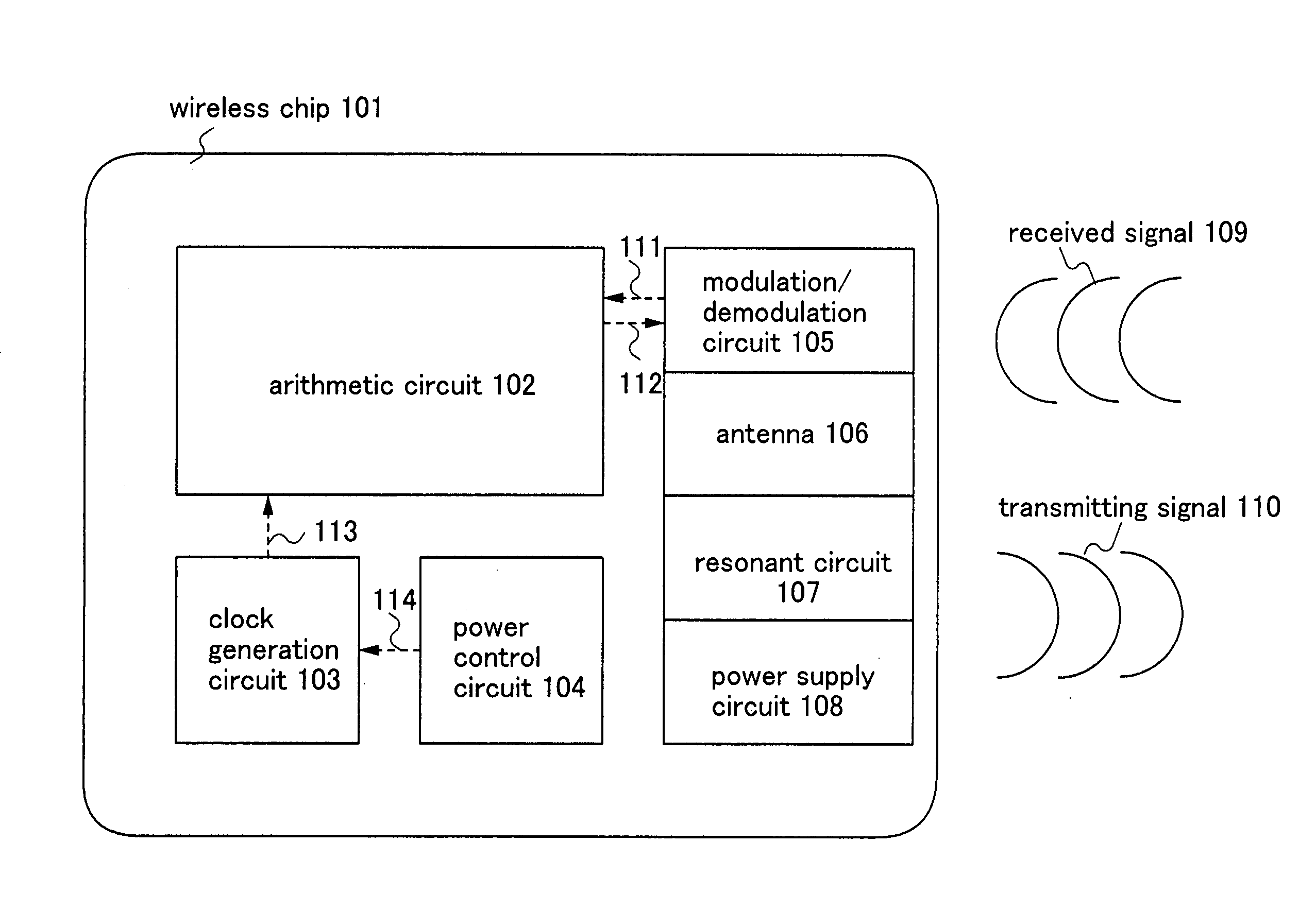
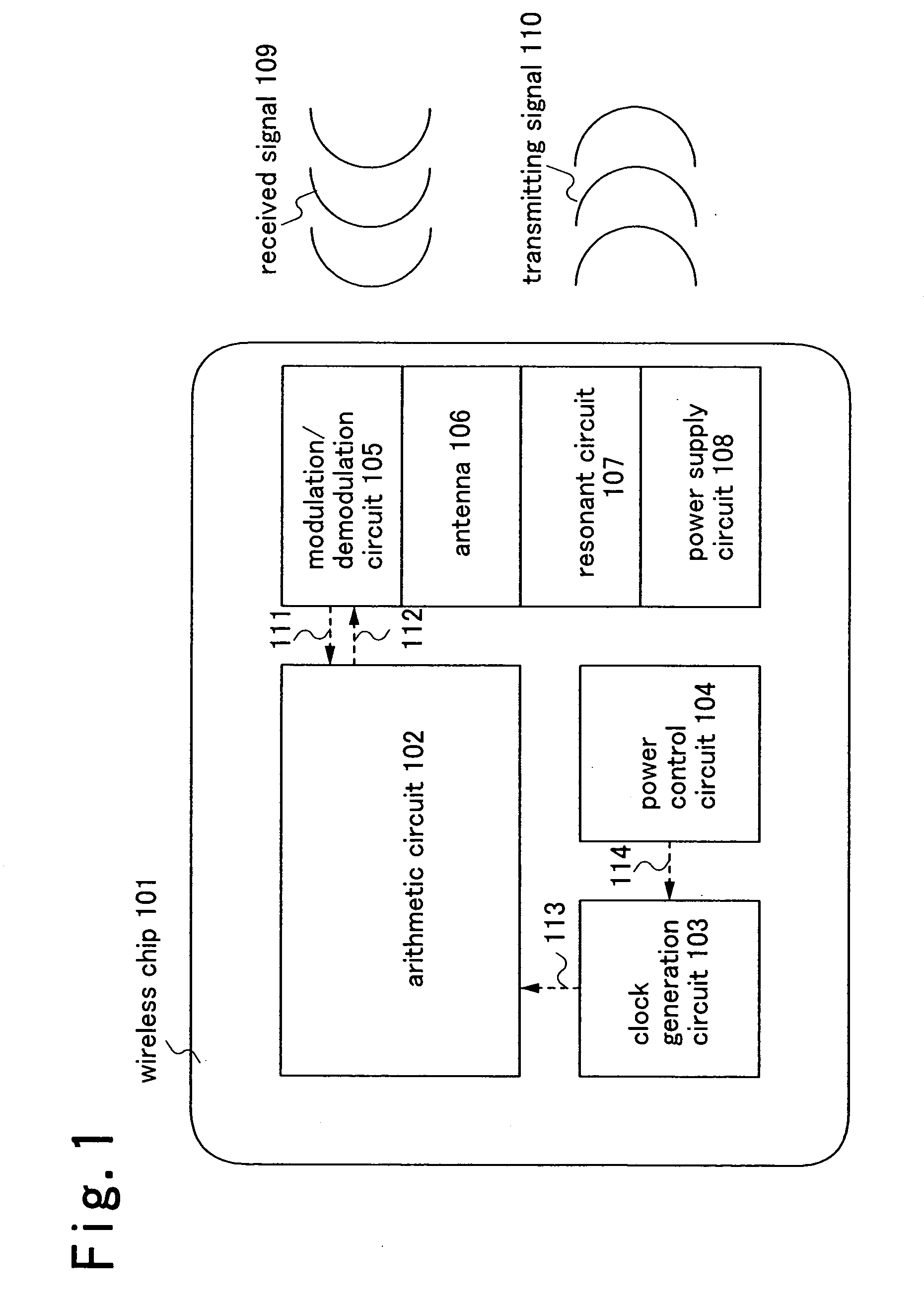
Therefore, in order to operate arithmetic circuits in the wireless chip, a large scale antenna or a large scale power supply circuit which can supply large current with communication signals, a clock generation circuit which can supply stable clock signals, and the like are required; further, increase in the area of a chip, rise in cost of a chip, and the like are concerns.
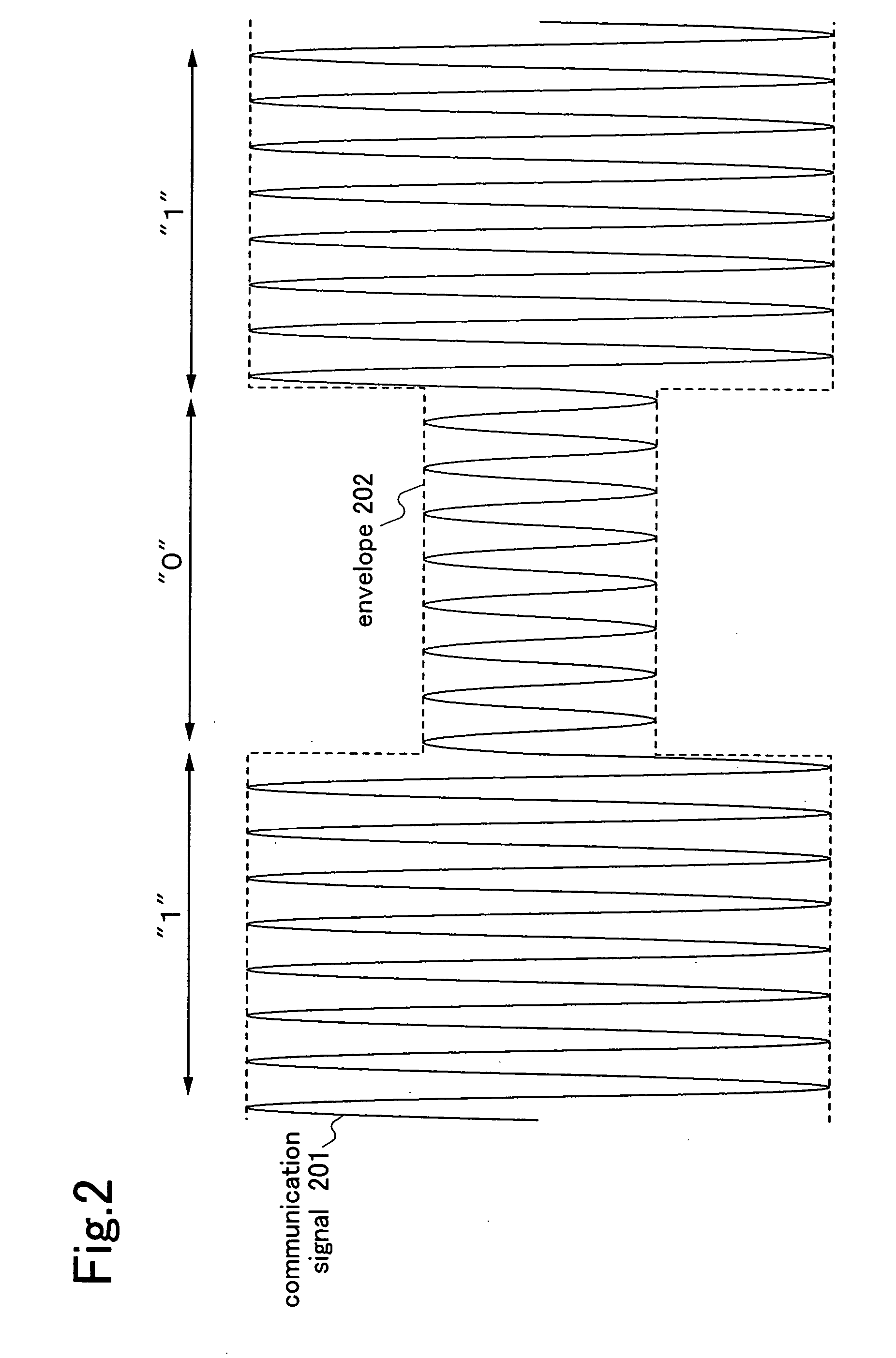
In addition, since the ASK system is used for data transmission, supply of supply voltage or a clock signal tends to be unstable when receiving “0”.
When the supply of supply voltage or clock signals becomes unstable, a malfunction occurs in a synchronous circuit.

Method used


Image

  • Semiconductor device
  • Semiconductor device
  • Semiconductor device

Examples


embodiment modes and embodiments

[0068] Embodiment modes and embodiments of the invention will be described below with reference to the drawings. Note that the invention is not limited to the following descriptions and it is easily understood by those skilled in the art that various changes may be made in modes and details without departing from the spirit and the scope of the invention. In the drawings for describing the embodiment modes embodiments, the same reference numerals are commonly given to like components, and the components will not be described repeatedly.

embodiment mode 1

[0069] As an embodiment mode of a semiconductor device of the present invention, first, FIG. 5 and FIGS. 6A and 6B show that the data racing in a synchronous circuit can be prevented by a non-overlapping clock. FIG. 5 shows a shift register as an example of a synchronous circuit included in a semiconductor device of the present invention. FIGS. 6A and 6B are timing charts of behavior of the shift register shown in FIG. 5. In FIG. 5, first to fourth latches 501 to 504 are connected in series. The first to fourth latches 501 to 504 are level sensitive latches for supplying first to fourth clock signals as gate signals respectively to first to fourth clock wirings 505 to 508. Accordingly, the first to fourth latches 501 to 504 respectively store voltage values of first to fourth data wirings 509 to 512 when the first to fourth clock signals supplied to the first to fourth clock wirings 505 to 508 are “1”, and the stored voltage values are outputted to second to fifth data wirings 510 t...

embodiment 1

[0091] In this embodiment, as an example of a power control circuit in the configuration described in the embodiment mode, a method of controlling clock signals by monitoring variation in supply voltage will be described with reference to FIG. 7 and FIG. 8. FIG. 7 shows a circuit diagram of a power control circuit in this embodiment. FIG. 8 is a flowchart showing behavior of a power control circuit in this embodiment.

[0092] First, a circuit diagram of a power control circuit of this embodiment will be described with reference to FIG. 7. In FIG. 7, an output terminal of a first regulator 701 is connected to a resistor 707, an output terminal of a second regulator 702 is connected to a resistor 709, and an output terminal of an nth regulator 703 is connected to a resistor 711. An input terminal of a first operational amplifier 719 is connected to resistors 707, 708, 713, and 714, and the output terminal is connected to the resistor 713 and a first digital buffer 722. An input termina...


PUM


Abstract

In a semiconductor device having a large-scale arithmetic circuit, when there is delay in clock signals, a malfunction occurs in a circuit. In particular, in an environment where supply voltage varies as in a wireless chip, it is very difficult to precisely estimate delays in clock signals in designing. Further, in order to keep supply voltage stable, a large-scale power supply circuit is required, which increases the area of a chip, and the cost thereof. A semiconductor device provided with a power control circuit and a clock generation circuit is used to detect variation in supply voltage using the power control circuit and changing frequency and duty ratio of a clock circuit using the clock generation circuit, thereby operating an arithmetic circuit stably. A high performance semiconductor device provided with such a large-scale arithmetic circuit can be provided at low cost.

Description

BACKGROUND OF THE INVENTION [0001] 1. Field of the Invention [0002] The present invention relates to a semiconductor device including a large scale arithmetic circuit, and particularly to a semiconductor device in which an arithmetic circuit can be operated stably even when supply voltage changes. Specifically, the present invention relates to a semiconductor device in which a large scale circuit having advanced arithmetic functions, to which supply voltage is supplied with a wireless communication signal is formed from semiconductor thin film transistors. [0003] 2. Description of the Related Art [0004] In recent years, a compact semiconductor device in which micro IC chips and an antenna for wireless communication are combined (hereinafter referred to as a wireless chip) is spotlighted. A wireless chip can write data or read data by transmitting / receiving communication signals (operation magnetic field) using a wireless communication device (hereinafter referred to as a reader / writ...

Claims


Application Information

Patent Timeline
Patent Type & Authority Applications(United States)
IPC IPC(8): G06F17/50
CPCG06F1/08H01L27/283H01L27/1203H01L27/105H10K19/10G11C5/14
Inventor KUROKAWA, YOSHIYUKI
Owner SEMICON ENERGY LAB CO LTD
Learn More