Etchant composition, methods of patterning conductive layer and manufacturing flat panel display device using the same

a flat panel display and composition technology, applied in the direction of crystal growth process, after-treatment details, other domestic articles, etc., can solve the problems of increasing manufacturing costs and manufacturing time, complicated etching process for forming tft and interconnections, and difficulty in etching respective conductive layers formed of different materials with the same etchant composition. , to achieve the effect of reducing manufacturing costs and simplifying the etching process

Active Publication Date: 2007-02-08
LG DISPLAY CO LTD
View PDF9 Cites 25 Cited by
  • Summary
  • Abstract
  • Description
  • Claims
  • Application Information

AI Technical Summary

Benefits of technology

[0012] An advantage of the present invention is to provide an etchant composition capable of simplifying an etching process and minimizing manufacturing costs, and methods of patterning a conductive layer and manufacturing a flat panel display device using the same.

Problems solved by technology

However, it is difficult to etch respective conductive layers formed of different materials with the same etchant composition because each of the conductive layers has an etching rate different from each other.
Thus, the etching process for forming the TFT and the plurality of interconnections is complicated, and manufacturing costs and manufacturing time increase.
This results in a decreased productivity.
However, an etchant which may simultaneously etch Al, Mo and ITO has not been developed.
Therefore, it is impossible to form the TFT and the pixel electrode using the same etchant composition.

Method used


Image

  • Etchant composition, methods of patterning conductive layer and manufacturing flat panel display device using the same
  • Etchant composition, methods of patterning conductive layer and manufacturing flat panel display device using the same
  • Etchant composition, methods of patterning conductive layer and manufacturing flat panel display device using the same

Examples


experimental example 1

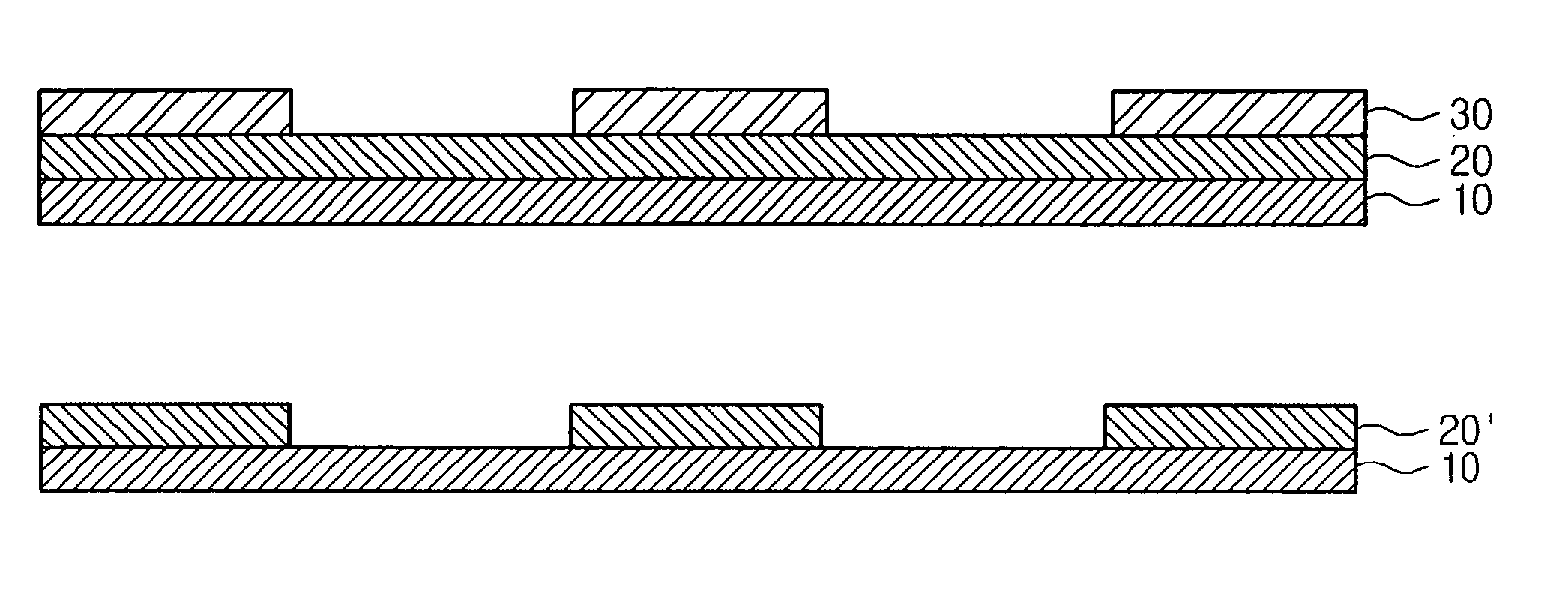
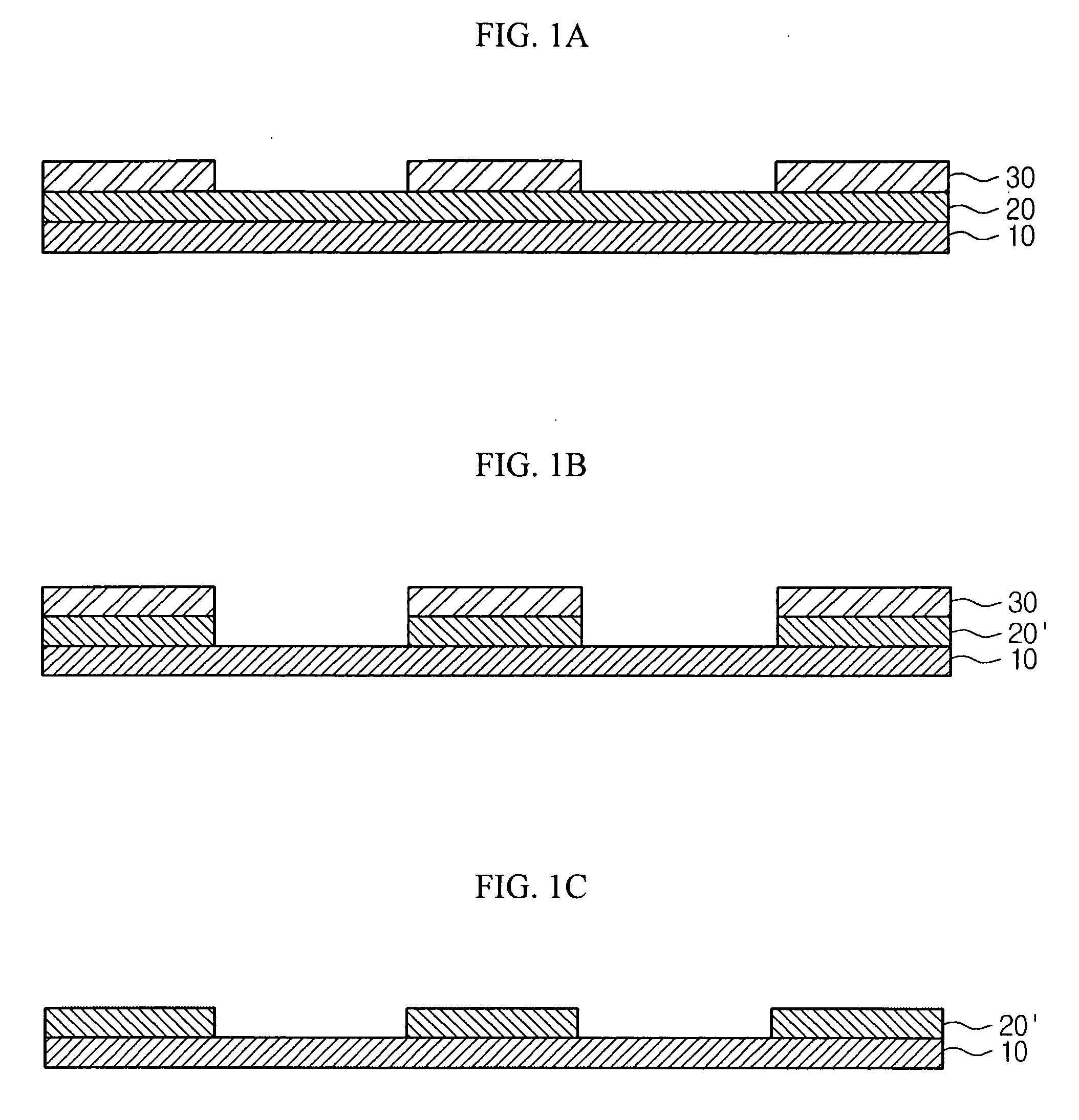
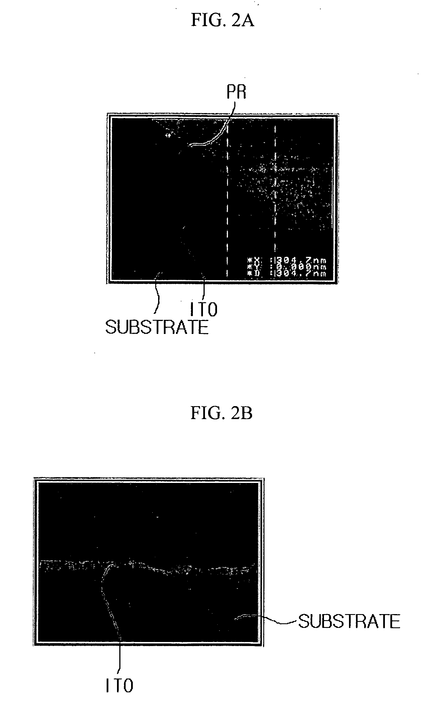
[0057] ITO is deposited on a substrate. Thereafter, after forming a photoresist layer on the ITO layer, exposure and development processes are performed so as to form a photoresist pattern exposing a portion of the ITO layer. Afterwards, after etching the exposed ITO layer using the etchant having a predetermined composition illustrated in Table 1 below, the photoresist pattern is removed to thereby form the ITO layer pattern. Sections before removing the photoresist patterns and sections after removing the photoresist pattern are observed by a scanning electron microscope (SEM) after etching the ITO layer into a predetermined configuration.

experimental example 2

[0058] The same processes as are performed except that Mo is deposited on the substrate to form a Mo single layer. Thus, the processes form a Mo single layer pattern.

experimental example 3

[0059] The same processes as are performed except that AlNd alloy and Mo are deposited on the substrate in sequence to form a Mo / AlNd bilayer. Thus, the processes form a Mo / AlNd bilayer pattern.


PUM

PropertyMeasurementUnit
concentrationaaaaaaaaaa
conductiveaaaaaaaaaa
organicaaaaaaaaaa

Abstract

An etchant composition, and methods of patterning a conductive layer and manufacturing a flat panel display device using the same are provided. The etchant composition may include phosphoric acid, nitric acid, acetic acid, water and an additive, wherein the additive includes a chlorine-based compound, a nitrate-based compound, and an oxidation regulator. In addition, the flat panel display device may be manufactured by patterning a gate electrode, source / drain electrodes and a pixel electrode using the same etchant composition. The gate electrode, source / drain electrodes and the pixel electrode may be formed of different conductive materials. Accordingly, processes are simplified so that manufacturing costs may be reduced and productivity may be improved.

Description

[0001] This application claims the benefit of Korean Patent Application No. 10-2005-0072338, filed in Korea on Aug. 8, 2005, which is hereby incorporated by reference for all purposes as if fully set forth herein. BACKGROUND OF THE INVENTION [0002] 1. Field of the Invention [0003] The present invention relates to an etchant composition, and methods of patterning a conductive layer and manufacturing a flat panel display device using the same. More particularly, the present invention relates to an etchant composition capable of simultaneously etching aluminum, molybdenum and indium-tin-oxide, and methods of patterning a conductive layer and manufacturing a flat panel display device using the same. [0004] 2. Description of the Related Art [0005] Flat panel display devices are generally classified into passive matrix type flat panel display devices and active matrix type flat panel display devices, according to the driving scheme employed in the flat panel display device. An active matr...

Claims


Application Information

Patent Timeline
Patent Type & Authority Applications(United States)
IPC IPC(8): C23F1/00B44C1/22C09K13/00
CPCC23F1/20C09K13/06H01L21/32134C23F1/26C23F1/02C09K13/04G03F7/20
Inventor LEE, KYOUNG MOOKSONG, KYE CHAN
Owner LG DISPLAY CO LTD
Why Eureka
Try Eureka