Supercharge Your Innovation With Domain-Expert AI Agents!

Method for growing silicon single crystal and silicon wafer

a single crystal and silicon wafer technology, applied in the direction of silicon compounds, silicates, etc., can solve the problems of deteriorating electrical properties, unable to be used as prime wafers, and generating cop and/or dislocation cluster defects, so as to increase the pull rate margin of a defect-free crystal, the effect of safe operation of the growing apparatus

Active Publication Date: 2007-02-15
SUMCO CORP
View PDF3 Cites 5 Cited by
  • Summary
  • Abstract
  • Description
  • Claims
  • Application Information

AI Technical Summary

Benefits of technology

[0026] In the present invention, the “Wright etching defect” means “a defect to be detected using an optical microscope after an As-Grown silicon wafer is subjected to the following treatment”. The silicon wafer is subjected to a cupper decoration in which the wafer is immersed into a copper sulfate solution, dried naturally and heat-treated at 900° C. for approximately 20 minutes in the nitrogen gas ambient. And then, in order to remove a Cu silicide layer in the surface layer of the wafer, the wafer is immersed into a mixed solution of HF / HNO3 so as to etch and remove the surface layer by tens of microns. Thereafter the wafer surface is subjected to a Wright-etching (cromic acid etching) by 2 microns. In accordance with this treatment and evaluation, the dislocation cluster defects formed during the crystal growth are exposed by the copper decoration, and the dislocation cluster defects can be detected with excellent sensitivity.
[0059] In accordance with the present invention, a silicon single crystal can be grown in which an LSTD density of LSTD of 0.09 μm or greater which is the dislocation cluster defect is low. Since in silicon wafers obtained using the grown silicon single crystal, the LSTD density is low and the LPD density of LPD of 0.09 μm or greater which is increased by repeating SC-1 cleaning 10 times is also low, the silicon wafers is suitably used as an LPD monitoring wafer.

Problems solved by technology

However, if the pull rate range is deviated even slighltly, there is the inconvenience that COP and / or dislocation cluster defects are generated.
In particular, a wafer where the dislocation cluster defects have been generated deteriorates the electrical properties of a device; thereby, it cannot be used as a prime wafer.
However, in accordance with the recent miniaturization of integrated circuits, the LPD size to be monitored has become smaller.

Method used


Image

  • Method for growing silicon single crystal and silicon wafer
  • Method for growing silicon single crystal and silicon wafer
  • Method for growing silicon single crystal and silicon wafer

Examples


examples

[0086] The following experiments were conducted in order to verify the present invention:

experimental examples 1 to 5

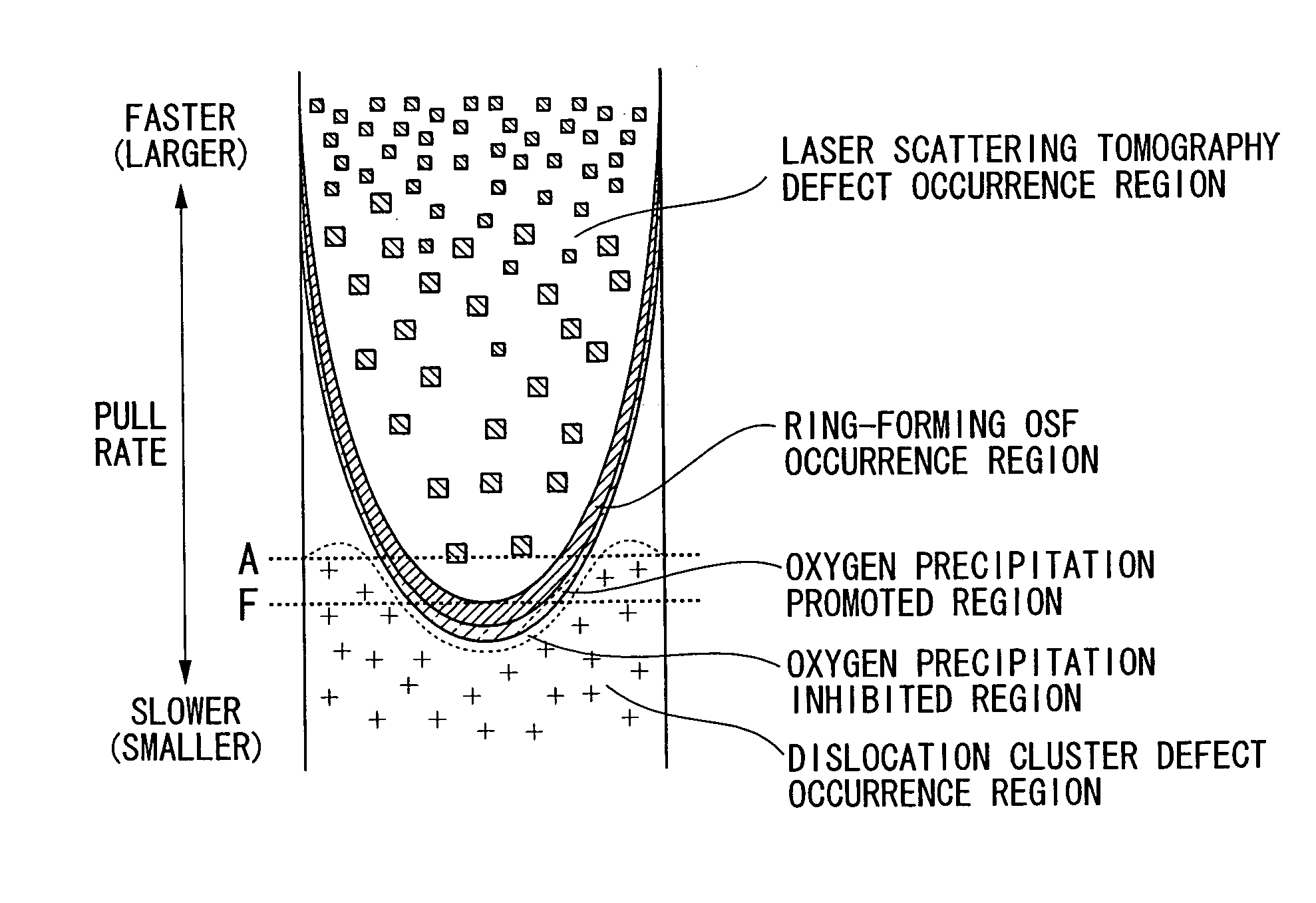
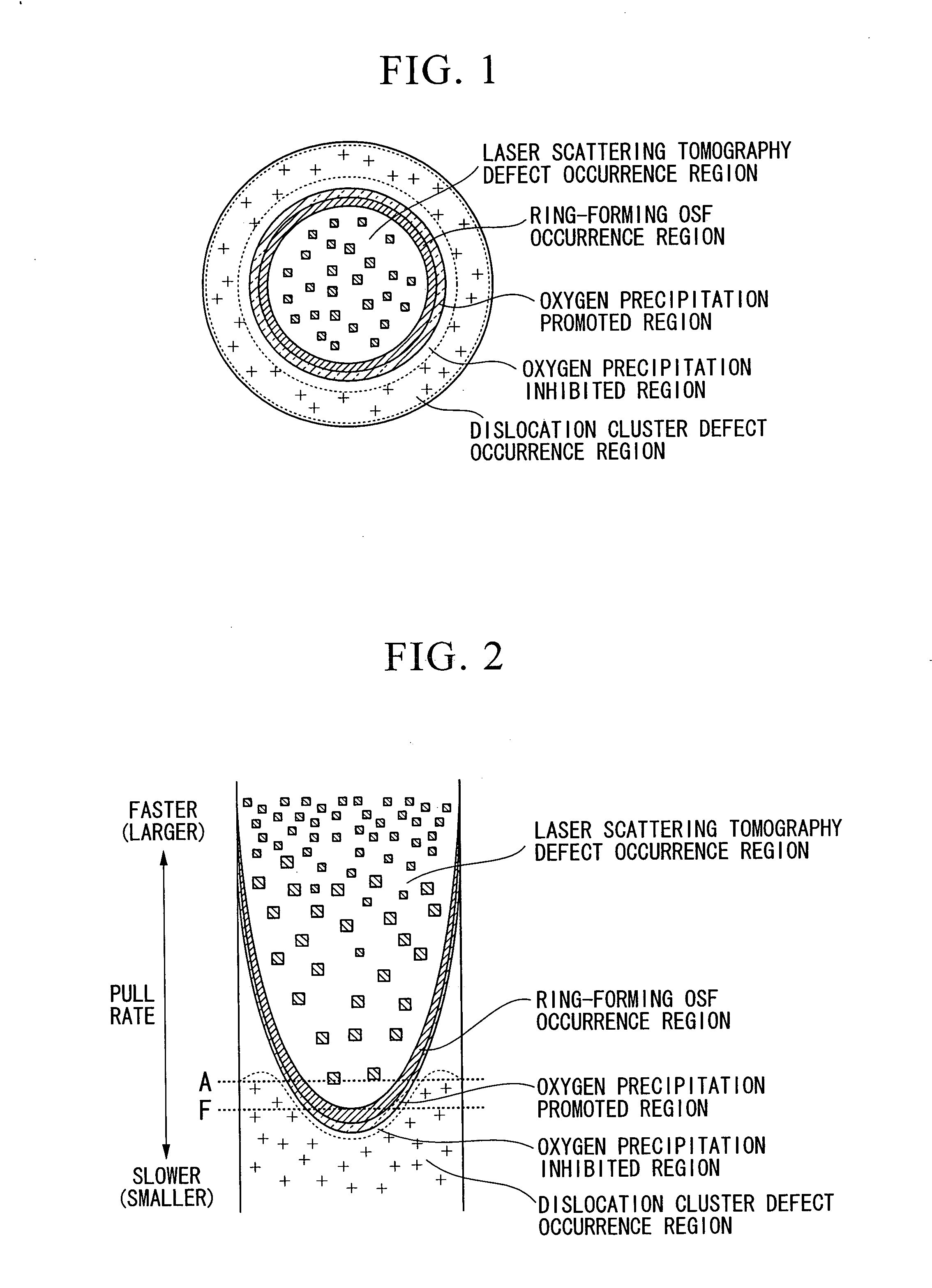
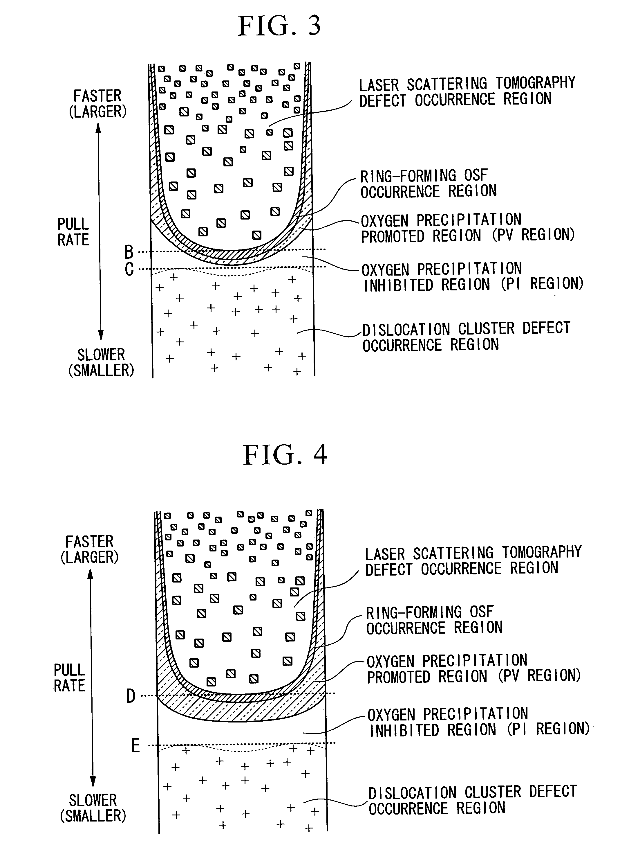
[0087] Using the apparatus for growing a single crystal having the hot zone structure where (Gc≧Ge), which is the same apparatus for growing a single crystal used when manufacturing the silicon single crystal in FIG. 3, an inert gas where hydrogen had been added was supplied to the growth furnace to establish the hydrogen partial pressure in Experimental examples 1 to 5 shown in Table 1, respectively, and the silicon single crystal was grown at the pull rate to establish 5×10⁴ / cm2 or greater of the Wright etching defect density on the radial cross section of the silicon single crystal, and 3×10⁴ / cm2 or greater of the Secco etching defect density, and the obtained silicon single crystal was sliced and silicon wafers in Experimental examples 1 to 5 were obtained, respectively.

[0088] Then, the LPD density of LPD of 0.09 μm or greater before and after 10 times of repetition of the SC-1 cleaning of the surface of the silicon wafers in Experimental examples 1 to 5 was obtained, respectiv...


PUM


Abstract

In this method for growing a silicon single crystal, an ambient gas where a single crystal is grown contains a gas hydrogen-containing substance, and a silicon single crystal is grown at a pull rate to form a dislocation cluster defect occurrence region at least in a portion of a radial cross section of said silicon single crystal and at a pull rate which is slower than that to form an laser scattering tomography defect occurrence region, according to the Czochralski method. This silicon wafer is sampled from a straight body of the silicon single crystal grown using said method for growing a silicon single crystal, and the LPD density of LPD of 0.09 μm or greater in the surface after 10 times of repetitions of the SC-1 cleaning is 0.1 / cm2 or less.

Description

BACKGROUND OF THE INVENTION [0001] 1. Field of the Invention [0002] The present invention relates to a method for growing a silicon single crystal and a silicon wafer, and particularly relates to a method for growing a silicon single crystal which enables the growth of a silicon single crystal including a dislocation cluster defect occurrence region having a low density of LPD (Light Point Defect) of 0.09 μm or greater. [0003] This application claims priority from Japanese Patent Application No. 2005-234034 filed on Aug. 12, 2005, the content of which is incorporated herein by reference. [0004] 2. Background Art [0005] As a method for manufacturing a silicon single crystal which is a starting material of a silicon wafer, a growing method in accordance with the Czochralski method (hereafter, referred to as “CZ method”) is known. [0006] It is known that minute defects which become exposed in a device manufacturing process, i.e., a grown-in defect is generated in the silicon single cry...

Claims


Application Information

Patent Timeline
IPC IPC(8): C30B15/00C30B21/06C30B27/02C30B28/10C30B30/04
CPCC30B15/04C30B29/06C30B15/203
Inventor ONO, TOSHIAKISUGIMURA, WATARUHOURAI, MASATAKA
Owner SUMCO CORP
Features
  • R&D
  • Intellectual Property
  • Life Sciences
  • Materials
  • Tech Scout
  • Unparalleled Data Quality
  • Higher Quality Content
  • 60% Fewer Hallucinations
Learn More