Semiconductor laser, optical element, laser device, and method of controlling semiconductor laser

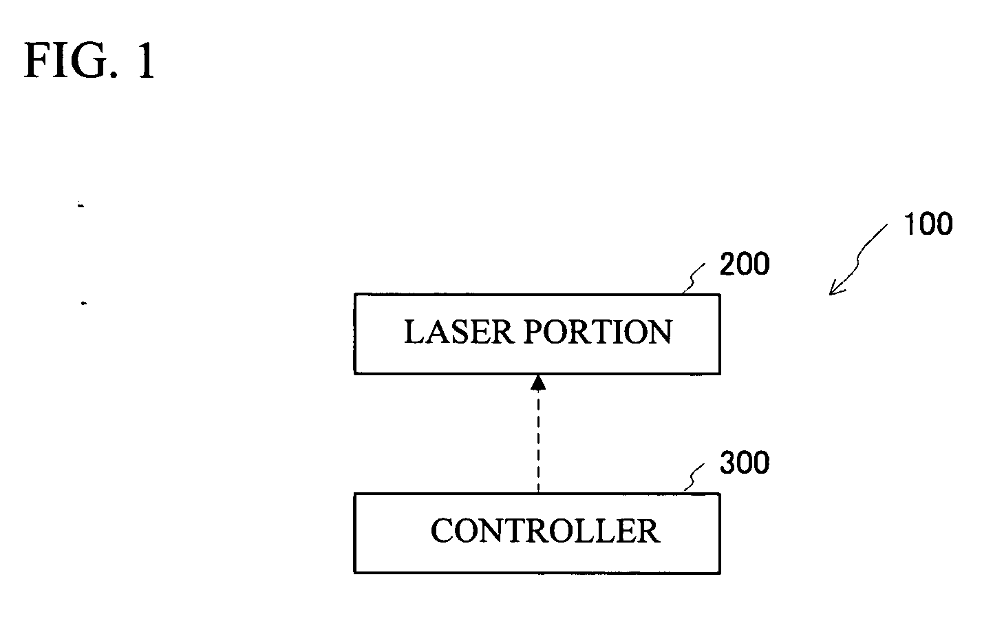
a laser device and semiconductor technology, applied in the direction of laser optical resonator construction, laser details, optical resonator shape and construction, etc., can solve the problems of stable laser emission of document 1, degraded mode stability of laser emission, and laser emission tends to be emitted, so as to reduce laser emission and facilitate the change of laser emission wavelength.

Active Publication Date: 2007-02-15
SUMITOMO ELECTRIC DEVICE INNOVATIONS
View PDF14 Cites 26 Cited by
  • Summary
  • Abstract
  • Description
  • Claims
  • Application Information

AI Technical Summary

Benefits of technology

[0028] With the above-mentioned configuration, a laser light is generated in the optical amplifier. And the light is provided in the first optical element. Peak reflection intensity of the optical longitudinal mode of the first diffractive grating area has wavelength dependence, because the optical lengths of at least two of the second areas are different from each other. In this case, the peak reflectivity of the optical longitudinal mode of the first diffractive grating area indicates relatively high in a given wavelength...

Problems solved by technology

However, it is difficult that the laser in Document 1 emits a stable laser, because the Q value of reflection spectrum of the simple FP resonator is small.
There is, therefore, a problem that the mode stability of the laser emission is degraded.
Accordingly, there is a problem that a laser tends to be emitted at the optical longitudinal mode next to the desirable frequency.
As mentioned above, there is a problem that an emission tends to occur at frequencies besides a desirable one and the mode stability of a laser emission is degraded in a conventional art, in a case where an element is structured so as to change a laser wavelength in a broad range.
That is, it is very difficult to restrain the mode degra...

Method used


Image

  • Semiconductor laser, optical element, laser device, and method of controlling semiconductor laser
  • Semiconductor laser, optical element, laser device, and method of controlling semiconductor laser
  • Semiconductor laser, optical element, laser device, and method of controlling semiconductor laser

Examples


second embodiment

(Second Embodiment)

[0078] Next, a description will be given of a laser device 100a in accordance with a second embodiment of the invention. The laser device 100a has a laser portion 200a instead of the laser portion 200, being different from the laser device 100 shown in FIG. 1. A description will be given of the laser portion 200a.

[0079]FIG. 7 illustrates a schematic cross sectional view of the laser portion 200a. The laser portion 200a has a Phase Shift (PS) area D between the Gain area B and the SG-DR area C, being different from the laser portion 200. The PS area D has a structure in which a waveguide core 15, the cladding layer 6, the contact layer 7 and an electrode 16 are laminated on the substrate 1.

[0080] The substrate 1 and the cladding layer 6 of the CSG-DR area A, the Gain area B, the PS area D and the SG-DR area C are formed as a unit respectively. The waveguide cores 3, 4, 5 and 15 are formed on a same plane and form one waveguide core together. The insulating layer ...

third embodiment

(Third Embodiment)

[0082] Next, a description will be given of a laser device 100b in accordance with a third embodiment. The laser device 100b has a laser portion 200b instead of the laser portion 200, being different from the laser device 100 shown in FIG. 1. A description will be given of the laser portion 200b.

[0083]FIG. 8A and FIG. 8B illustrate a detail of the laser portion 200b. FIG. 8A illustrates a top view of the laser portion 200b. FIG. 8B illustrates a cross sectional view taken along a line B-B of FIG. 8A. A description will be given, with reference to FIG. 8A and FIG. 8B, of the laser portion 200b. The laser portion 200b has the PS area D, a SG-DFB area E and a Power Control (PC) area F instead of the Gain area B and the SG-DR area C.

[0084] The laser portion 200b has a structure in which the CSG-DR area A, the PS area D, the SG-DFB area E and the PC area F are coupled in order. The SG-DFB area E has a structure in which a waveguide core 17, the cladding layer 6, the c...

fourth embodiment

(Fourth Embodiment)

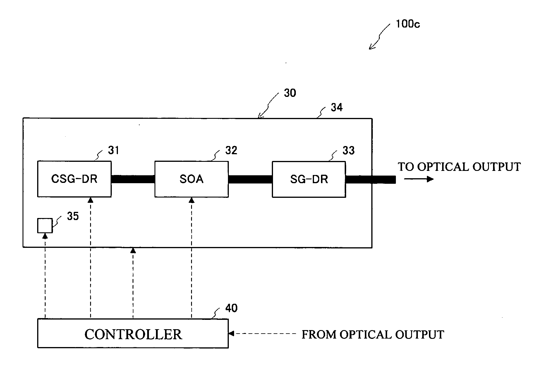
[0091] Next, a description will be given of a laser device 100c in accordance with a fourth embodiment. FIG. 9 illustrates an entire structure of the laser device 100c. As shown in FIG. 9, the laser device 100c has a laser module 30 and a controller 40. The laser module 30 has an optical element 31, a light amplifacation portion 32, an optical element 33, a temperature control device 34 and a thermistor 35. The optical element 31, the light amplification portion 32 and the optical element 33 are arranged on the temperature control device so as to form an optical axis.

[0092] The optical element 31 is an optical element having the CSG-DR area A mentioned above. The optical element 33 is an optical element having the SG-DR area C mentioned above. The light amplification portion 32 receives an instruction from the controller 40, amplifies an input light having a given effective wavelength range, and outputs a laser light. The laser light output from the amplification...


PUM


Abstract

A semiconductor laser has a first diffractive grating area. The first diffractive grating area has a plurality of segments. Each segment has a first area including a diffractive grating and a second area that is space area combined to the first area. Optical lengths of at least two of the second areas are different from each other. A refractive-index of each of the segments are changeable.

Description

BACKGROUND OF THE INVENTION [0001] 1. Field of the Invention [0002] This invention generally relates to a semiconductor laser, an optical element, a laser device, and a method of controlling the semiconductor laser. [0003] 2. Description of the Related Art [0004] Many organizations have developed a wavelength changeable semiconductor laser having an element which can emit various wavelengths laser lights, as Wavelength Division Multiplexing (WDM) communication using an optical fiber has been spread. The wavelength changeable semiconductor lasers proposed before now are classified broadly into a semiconductor laser having a Semiconductor Optical Amplifier (SOA) in an external resonator thereof and controlling an emitting wavelength with a wavelength selecting mechanism in the external resonator and a semiconductor laser having a structure in which a resonator acting as a wavelength selectable portion is built in a semiconductor element amplifying a laser light. [0005] A laser having ...

Claims


Application Information

Patent Timeline
IPC IPC(8): H01S5/00H01S3/08H01S5/12
CPCH01S5/0265H01S5/12H01S5/0425H01S5/0612H01S5/06256H01S5/1057H01S5/106H01S5/1064H01S5/1209H01S5/1212H01S5/1221H01S5/1231H01S5/124H01S5/1246H01S5/125H01S5/0287
Inventor FUJII, TAKUYA
Owner SUMITOMO ELECTRIC DEVICE INNOVATIONS
Why Eureka
Try Eureka