Semiconductor device

Inactive Publication Date: 2007-02-22
RENESAS ELECTRONICS CORP
View PDF5 Cites 20 Cited by
  • Summary
  • Abstract
  • Description
  • Claims
  • Application Information

AI Technical Summary

Benefits of technology

[0014] According to the present invention, a packaging structure, which can achieve both the improvement of the radiation performance and the mass productivity in the manufacturing process in the case where

Problems solved by technology

Further, since the numbers of components, required connecting members, and packaging processes thereof are increased by adding the heat spreader, the cost of a product is increased.
On the other hand, the conventional technology disclosed in the Patent Document 2 also has the problems as follows.
That is, although the effect of reducing the thermal resistance can be expected from the flip chip packaging, since a thick interlayer insulating film is provided between a main heat generating area of a semiconductor element and heat radiation bump, the thermal resistance reducing effect is limited.
Also, when the heat radiation bump and the electrical conne

Method used


Image

  • Semiconductor device
  • Semiconductor device
  • Semiconductor device

Examples


first embodiment

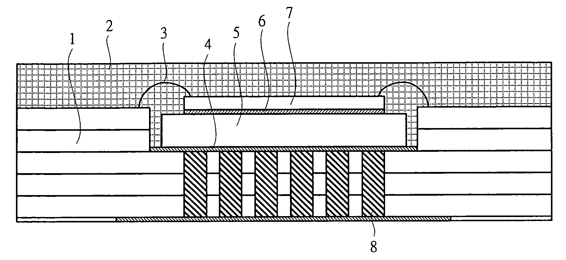
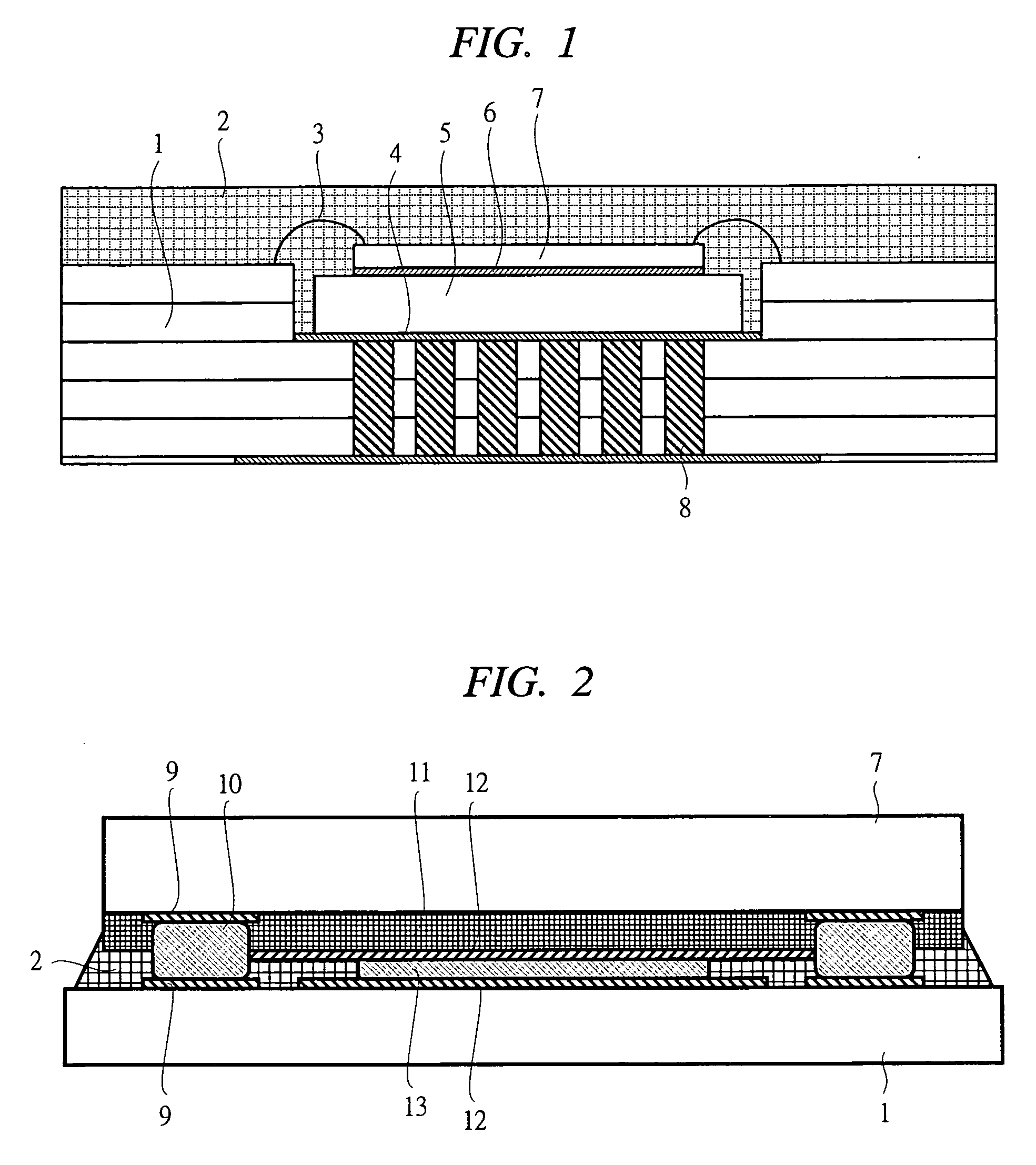
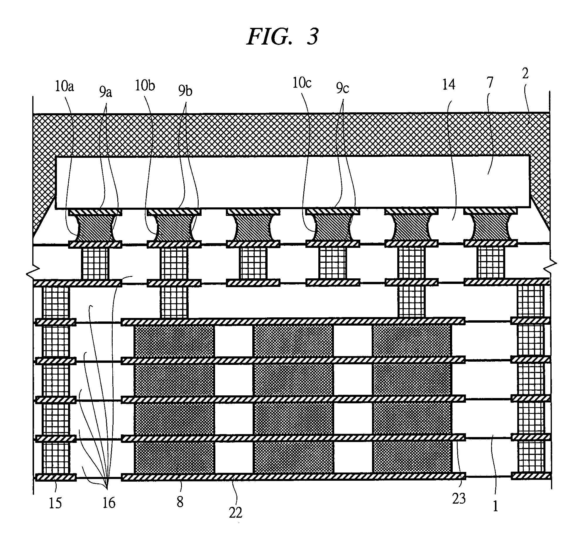
[0043] A semiconductor device according to the present invention will be described with reference to FIG. 3 to FIG. 9. FIG. 3 is a cross-sectional view showing a packaging structure of a semiconductor device. FIG. 4 is a diagram showing the layout of element bump electrodes in the semiconductor device. FIG. 5 is a cross-sectional view showing a connection structure from an active area to a circuit board in the semiconductor device. FIG. 6 is a cross-sectional view showing a packaging structure of the semiconductor device in which thermal vias are formed in the second and lower layers of the circuit board. FIG. 7 is a cross-sectional view showing another connection structure from an active area to a circuit board in the semiconductor device. FIG. 8 is a cross-sectional view showing still another connection structure from an active area to a circuit board in the semiconductor device. FIG. 9 is a cross-sectional view showing a connection structure from an active area to a thermal via i...

second embodiment

[0054] A semiconductor device according to the second embodiment of the present invention will be described with reference to FIG. 10 to FIG. 13. FIG. 10 is a diagram showing an example where source electrodes are closely aligned in the layout of the element bump electrodes in the semiconductor device. FIG. 11 is a cross-sectional view showing the connection structure from an active area to a thermal via in the wiring layers on the source or emitter side in the semiconductor device. FIG. 12 is a cross-sectional view showing another connection structure from an active area to a thermal via in the wiring layers on the source or emitter side in the semiconductor device. FIG. 13 is a cross-sectional view showing still another connection structure from an active area to a thermal via in the wiring layers on the source or emitter side in the semiconductor device. Note that the cross-sectional structures of the semiconductor device of this embodiment which do not overlap with FIG. 10 to FI...

third embodiment

[0059] A semiconductor device according to the third embodiment of the present invention will be described with reference to FIG. 14 to FIG. 18. FIG. 14 is a diagram showing an example where source electrodes are united to form a strip-shaped electrode in the layout of the element bump electrodes in a semiconductor device. FIG. 15 is a cross-sectional view showing a connection structure from an active area to a thermal via in the wiring layers on the source or emitter side in the semiconductor device. FIG. 16 is a cross-sectional view showing another connection structure from an active area to a thermal via in the wiring layers on the source or emitter side in the semiconductor device. FIG. 17 is a cross-sectional view showing still another connection structure from an active area to a thermal via in the wiring layers on the source or emitter side in the semiconductor device. FIG. 18 is a perspective view showing the positional relation between the bump electrode and the active area...


PUM


Abstract

A semiconductor device capable of reducing the thermal resistance in a flip chip packaging structure while achieving both the high radiation performance and manufacturing readiness without increasing the manufacturing cost is provided. In a semiconductor device having a semiconductor circuit for power amplification and a control circuit of the semiconductor circuit laminated on a multilayer circuit board, the semiconductor circuit for power amplification and the control circuit are aligned in parallel on the same semiconductor element, and the semiconductor element is flip-chip connected on the multilayer circuit board. Further, a second semiconductor element mounted in addition to the first semiconductor element and all components and submodules are flip-chip connected. Also, a plurality of bumps are united in order to improve the radiation performance and thermal vias of the multilayer circuit board are formed in second and lower layers of the wiring layers in the multilayer circuit board.

Description

CROSS-REFERENCE TO RELATED APPLICATION [0001] The present application claims priority from Japanese Patent Application No. JP 2005-235638 filed on Aug. 16, 2005 and Japanese Patent Application No. JP 2006-093000 filed on Mar. 30, 2006, the contents of which are hereby incorporated by reference into this application. TECHNICAL FIELD OF THE INVENTION [0002] The present invention relates to a technology effectively applied to a thermal design of a semiconductor device for a radio-frequency transmitter and receiver module and a semiconductor power supply mounted in a personal digital assistant such as a cellular phone. BACKGROUND OF THE INVENTION [0003] As a technology for a thermal design of a power semiconductor device for a radio-frequency transmitter and receiver module mounted in a personal digital assistant such as a cellular phone, a packaging structure for reducing its thermal resistance is disclosed in Japanese Patent Application Laid-Open Publication No. 2001-102483 (Patent Do...

Claims


Application Information

Patent Timeline
IPC IPC(8): H01L23/02
CPCH01L23/3677H01L23/49822H01L24/32H01L24/81H01L25/16H01L2224/16225H01L2224/16227H01L2224/48091H01L2224/48227H01L2224/73204H01L2224/73265H01L2224/81801H01L2924/10329H01L2924/15153H01L2924/1517H01L2924/00014H01L24/48H01L2924/01033H01L2924/0132H01L2924/01031H01L2224/32225H01L2924/00H01L2224/16235H01L2924/1305H01L2924/181H01L2924/00012H01L2224/45015H01L2924/207H01L2224/2612H01L2924/19105H01L2224/45099
Inventor OSONE, YASUOYORITA, CHIKOKAWANO, KENYAHASEGAWA, YUSHIRAI, YUJITOMOI, SEIICHIENDOU, TSUNEOKONISHI, SATORUNAKAJIMA, HIROKAZU
Owner RENESAS ELECTRONICS CORP
Why Eureka
Try Eureka