Semiconductor memory device

a memory device and semiconductor technology, applied in semiconductor devices, digital storage, instruments, etc., can solve the problems of difficult stably holding data, remarkable deterioration in worst value of snm, and risk of corruption of stored data, so as to prevent data corruption, reduce memory cell dimension, and prevent data corruption

Inactive Publication Date: 2007-02-22
NEC CORP
View PDF16 Cites 18 Cited by
  • Summary
  • Abstract
  • Description
  • Claims
  • Application Information

AI Technical Summary

Benefits of technology

[0012] The present invention has been completed with a view to addressing the above issues and has an object to provide a static random access memory (SRAM) that even when needed to operate at a ultra-speed with ultra-low voltage, can be realized in a reduced memory cell dimension using a memory cell composed of a minimum number of transistors for preventing corruption of stored data caused during the read operation.
[0013] According to the present invention, the memory cell of the static random access memory (SRAM) comprises first and second inverter circuits connected in loop to form a storage circuit and a storage control circuit serially connected to a drive transistor of the second inverter circuit to be operative to allow the first and second inverter circuits connected in loop to form the storage circuit for statically storing data when the memory cell is inactivated whereas when the memory cell is activated, a loop connection of the first and second inverter circuits is disconnected to dynamically store data. Dynamically storing data during the activation of the memory cell enables the prevention of corruption of data caused by read operation.
[0014] Further, causing a second access transistor connected to an output of the second inverter circuit to reset the output of the second inverter circuit to a low voltage potential during write operation allows the writ operation to be easily performed whereby the memory cell can be constructed of a less number of transistors with reduced number of control signals.
[0015] Furthermore, data transfer between a memory cell and a sense amplifier is efficiently performed using a sense amplifier applied with cell data from the memory cell through a single bit line. The memory cells are placed in layout in an L-shaped region and inverted in mirror such that a cell array configuration has a vacant space in such a region. Separately placing sense amplifiers in the vacant space enables a cellblock to be formed in a small surface area in an efficient manner.

Problems solved by technology

However, in an event that the word line signal WL is accessed to be raised to a high voltage potential, the data storage nodes V1, V2 and bit line pair BLT, BLN are made conductive to each other via access transistors to cause the low voltage potential of the data storage nodes V1, V2 to be raised from a ground potential, resulting in a difficulty of stably holding data.
Accordingly, remarkable deterioration occurs in a worst value of the SNM.
With the channel length of a value of 50 nm as shown, the worst value of the SNM becomes a value less than “0” and, hence, stored data has a risk of being corrupted when read operation is executed and a word line signal goes to a high voltage potential.
As disclosed in Literature 1 stated above, with the related art SRAM using six transistors, deterioration occurs in the worst value of the SNM, causing a difficulty to occur in stable data storage as a future possibility.
This causes a voltage potential of the data storage node to be inverted as shown in FIG. 6(C), causing corruption of data to occur.

Method used


Image

  • Semiconductor memory device
  • Semiconductor memory device
  • Semiconductor memory device

Examples


first embodiment

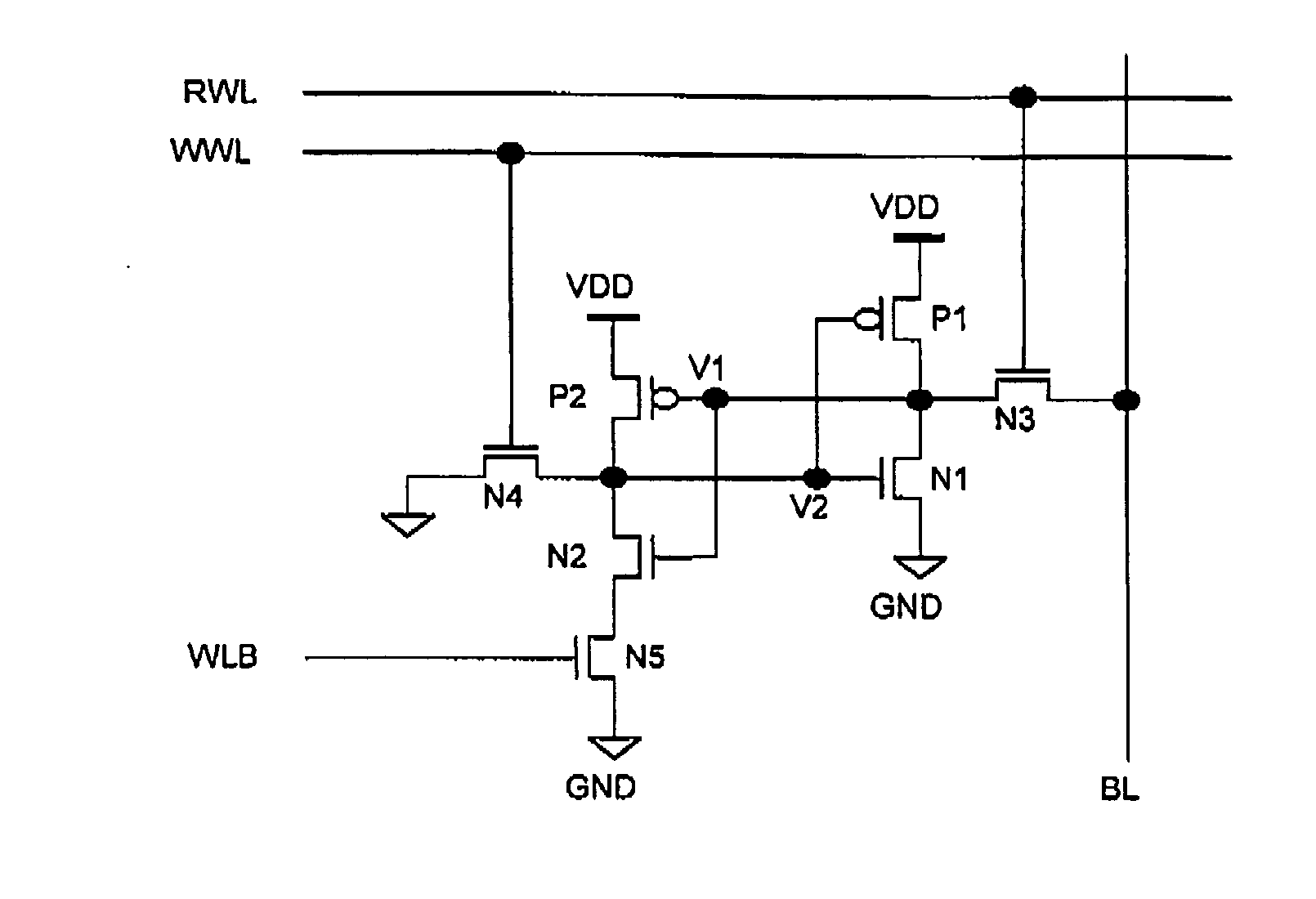
[0068] A first embodiment according to the present invention is described with reference to FIGS. 7 to 9. FIG. 7 shows a circuit structure representing an SRAM cell of a static random memory of the first embodiment. FIG. 8 is shown a timing chart for read operation, (A) is shown the reading “0” and (B) is shown the reading “1”. FIG. 9 is shown a timing chart for write operation, (A) is shown the writing “0” and (B) is shown writing “1”.

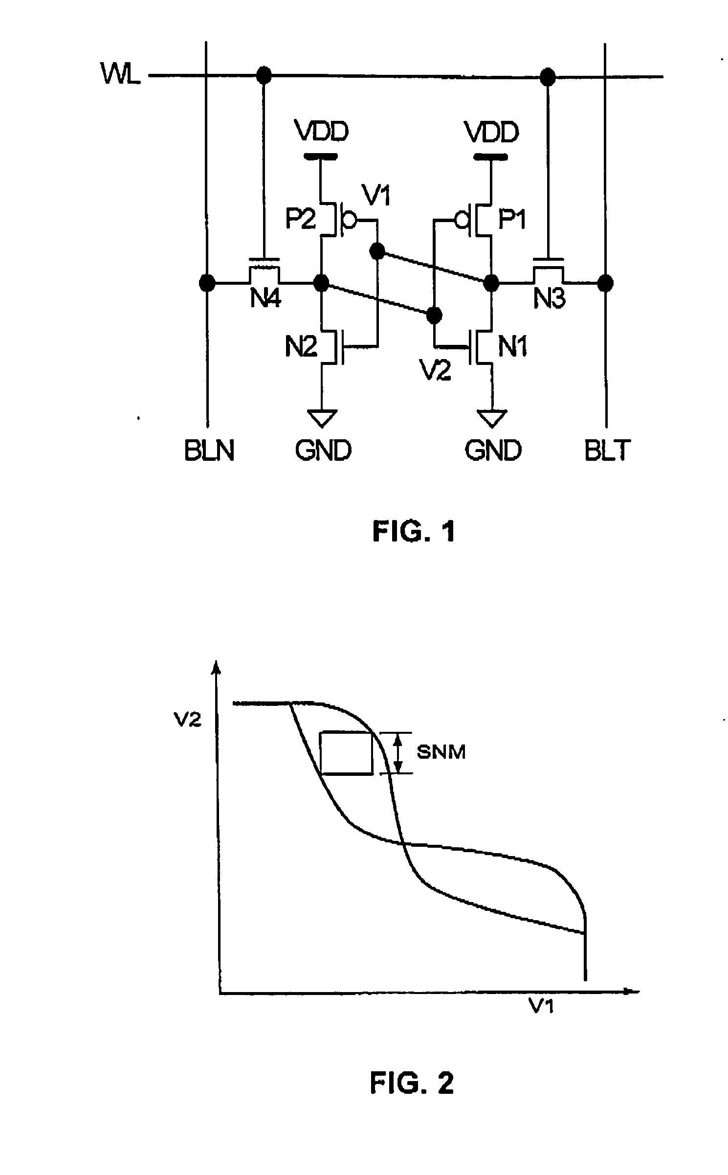
[0069] The RAM cell, shown in FIG. 7, is comprised of seven transistors including a PMOS transistor P1 and an NMOS transistor N1 by which a first CMOS inverter is formed, a PMOS transistor P2 and an NMOS transistor N2 by which a second CMOS inverter is formed, NMOS transistors N3 and N4 playing a role as access means, and an NMOS transistor N5 playing a role as a storage control means. Here, the PMOS transistors P1, P2 form the inverter circuit to play a role as load transistors and the NMOS transistors N1, N2 play a role as drive transistors.

[0070]...

second embodiment

[0083] A second embodiment according to the present invention will be described with reference to FIG. 10. FIG. 10 is a view showing a circuit structure of a memory cell of an SRAM of the second embodiment according to the present invention. The second embodiment corresponds to a case wherein a connected position of the storage control transistor N5 in the memory cell of the SRAM of the first embodiment is altered and has the same structure as that of the first embodiment in other circuit structures. While with the first embodiment, the storage control transistor N5 is inserted to the source side of the drive transistor N2, the second embodiment allows the storage control transistor N5 to be inserted to the drain side of the drive transistor N2.

[0084] The SRAM cell of the second embodiment, shown in FIG. 10, is comprised of seven transistors including a PMOS transistor P1 and an NMOS transistor N1 by which a first CMOS inverter is formed, a PMOS transistor P2 and an NMOS transistor...

third embodiment

[0088] A third embodiment according to the present invention is described with reference to FIGS. 11 to 13. FIG. 11 is a view showing a circuit structure of a memory cell of an SRAM of the third embodiment. FIG. 12 is a time chart showing first operation timings and FIG. 13 is a time chart showing second operation timings.

[0089] The SRAM cell, shown in FIG. 11(A), is comprised of seven transistors including a PMOS transistor P1 and an NMOS transistor N1 by which a first CMOS inverter is formed, a PMOS transistor P2 and an NMOS transistor N2 by which a second CMOS inverter is formed, NMOS transistors N3 and N4 playing a role as an access means, and an NMOS transistor N5 playing a role as a storage control means.

[0090] The first CMOS inverter is comprised of the PMOS transistor P1 and the NMOS transistor N1 and applied with data appearing at the data storage node V2 as an input, thereby outputting data at a data storage node V1. The second CMOS inverter is comprised of the PMOS tran...


PUM


Abstract

The SRAM cells of a semiconductor storage device each comprise first and second inverter circuits loop-connected with each other to form a hold circuit; two access transistors; and a hold control transistor connected in series with a drive transistor of the second inverter circuit. While the memory cell is not accessed, the hold control transistor causes the first and second inverter circuits to form the loop connected hold circuit for statically holding data. When the memory cell is accessed, the hold control transistor causes the first and second inverter circuits to be disconnected from the loop connection for dynamically holding data, thereby preventing data corruption that would otherwise possible occur due to a read operation. Moreover, a sense amplifier circuit that uses a single bit line to read data from a memory cell is disposed in a space appearing in the memory cell array, thereby effectively using the area.

Description

TECHNICAL FIELD [0001] The present invention relates to semiconductor memory devices and, more particularly, to a semiconductor memory device comprising a minimum number of transistors, operating at an ultra-high speed and an ultra-low voltage, preventing data corruption during the read operation. BACKGROUND POTENTIAL ART [0002] With custom ICs for use in an ASIC (Application Specific Integrated Circuit) or the like, attempts have heretofore been taken to refine transistors to the lower a power supply voltage for thereby improving operating speeds. With these custom ICs, a variety of memory devices are embedded. A need also arises for these embedded memory devices to similarly operate at the high speed and low power supply voltages and, in application to, for instance, cash memories or the like, a static random access memory (SRAM: Static Random Access Memory that is herein after referred to as SRAM) similarly needs to operate at the high speed and low power supply voltages. [0003] ...

Claims


Application Information

Patent Timeline
Patent Type & Authority Applications(United States)
IPC IPC(8): G11C11/00G11C11/41G11C11/412H01L27/10H01L27/11
CPCG11C11/412H01L27/11H10B10/00
Inventor TAKEDA, KOICHI
Owner NEC CORP
Why Eureka
Try Eureka