Micronized semiconductor nanocrystal complexes and methods of making and using same

Inactive Publication Date: 2007-03-01
EVIDENT TECH
View PDF32 Cites 82 Cited by
  • Summary
  • Abstract
  • Description
  • Claims
  • Application Information

AI Technical Summary

Benefits of technology

[0019] The ability to control the size of micronized nanocrystal complexes of the present invention through known grinding, milling and sieving techniques, allow the micronized particles to be used to trace the flow of a liquid, such as water. Whereas most filters are unable to filter semiconductor nanocrystals in a liquid, micronized semiconductor nanocrystal complexes of the present invention allow the size of the particles to be controlled to ensure that the majority of the particles are trapped by a filtration system.
[0020] Furthermore, the ability to control the size of micronized semiconductor nanocrystal complexes of the present invention also has advantages with respect to lighting applications. Traditional semiconductor nanocrystals when uniformly dispersed throughout a solution or matrix do not scatter light due to their extremely small size. Some lighting applications using phosphors require scattering to ensure an optimized absorbance and optimized white light emission. Micronized semiconductor nanocrystal complexes, according to the present invention, can ensure isotropic light emission. Additionally, electroluminescent displays may be made by using a transparent conductor (such as ITO), a bottom electrode of metal (conductor) and micronized semiconductor nanocrystal complexes of the present invention. In these electroluminescent displays, the micronized semiconductor nanocrystal complexes may be dispersed in the transparent conductor.
[0021] Micronized semiconductor nanocry

Problems solved by technology

Furthermore, a plurality of semiconductor nanocrystals placed in a micronized first matrix material may be hermetically sealed from the environment,

Method used


Image

  • Micronized semiconductor nanocrystal complexes and methods of making and using same
  • Micronized semiconductor nanocrystal complexes and methods of making and using same
  • Micronized semiconductor nanocrystal complexes and methods of making and using same

Examples


example 1

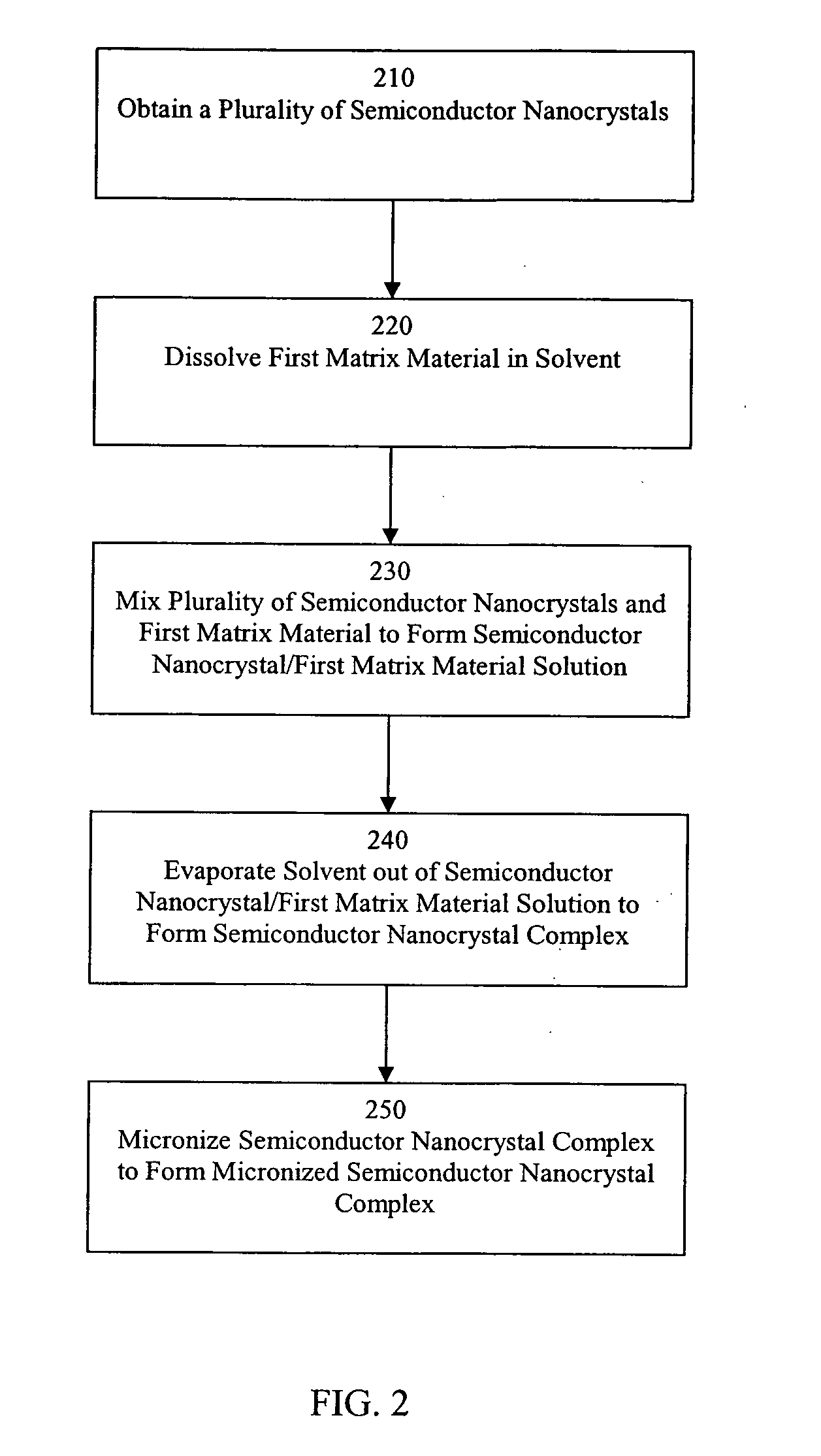
[0057] The following example describes a process for preparing a micronized semiconductor nanocrystal complex comprising a plurality of PbS semiconductor nanocrystals in a first matrix material that is polystyrene, wherein the polystyrene is micronized.

[0058] PbS semiconductor nanocrystals are purchased in toluene (Evident Technologies, Troy, N.Y.). 99 g of polystyrene is dissolved in 1.0 L of toluene at 110.6° C. (boiling). After the polystyrene is dissolved, 1.0 g of PbS semiconductor nanocrystals are added to the solution and mixed. Next, the toluene is evaporated by heating the solution to 110.6° C. until the total volume is reduced to approximately 500 mL. The solution is then poured into a 9×13 inch Pyrex tray, and placed in a fume hood overnight to allow for most of the solvent to evaporate. The remaining solvent is removed using a vacuum oven (50° C.) resulting in formation of a polymer / semiconductor nanocrystal solid. This resulting solid is then be processed in a blender ...

example 2

[0059] The following example describes a process for preparing a micronized semiconductor nanocrystal complex comprising a plurality of two different semiconductor nanocrystals (PbS and CdSe / ZnS nanocrystals) dispersed in a first matrix material that is polystrene.

[0060] PbS and CdSe / ZnS nanocrystals are purchased in toluene (Evident Technologies, Troy, N.Y.). 99 g of polystyrene are dissolved in 1.0 L of toluene at 110.6° C. (boiling). After the polystyrene is dissolved, 0.5 g of PbS semiconductor nanocrystals and 0.5 g of CdSe / ZnS nanocrystals are added to the solution and mixed. Next, the toluene is evaporated by heating the solution to 110.6° C. until the total volume is reduced to approximately 500 mL. The solution is then be poured into a 9×13 inch Pyrex tray, and placed in a fume hood overnight to allow most of the solvent to evaporate. The remaining solvent is removed using a vacuum oven (50° C.) resulting in formation of a polymer / semiconductor nanocrystal solid. This resu...

example 3

[0061] The following example describes a process for preparing a micronized semiconductor nanocrystal complex comprising a plurality of semiconductor nanocrystals dispersed in a first matrix material that is a sol-gel matrix.

[0062] CdSe / ZnS nanocrystals are purchased in toluene (Evident Technologies, Troy, N.Y.). A sol-gel material is prepared by combining 1.2 g of colloidal silica (Highlink OG 108-32) with 0.5 g of an amine modified acrylate oligomer (Sartomer CN371) and 0.1 g of 1-hydroxycyclohexylphenyl ketone. The solution is sonicated until the solution is clear. While that solution is being prepared, 17 mg of CdSe / ZnS nanocrystals are precipitated from toluene by adding methanol. 1.7 mL of the sol-gel solution is added to the precipitated CdSe / ZnS nanocrystals, and the mixture is sonicated until forming a homogeneous solution. Under a nitrogen atmosphere (glove-bag), the solution is applied on the surface of a polycarbonate sheet, and the solution is cured using a curing lamp...


PUM


Abstract

A micronized semiconductor nanocrystal complex including a plurality of semiconductor nanocrystals embedded in a first matrix material wherein the first matrix material is a micronized polymer. The micronized semiconductor nanocrystal complex can be used in or include inks, paints, dyes, LEDs, taggants, tracers and cosmetics. The present application further provides methods of making micronized semiconductor nanocrystal complexes.

Description

CROSS-REFERENCE TO RELATED APPLICATIONS [0001] The present application claims priority to U.S. Provisional Application No. 60 / 585,942, filed Jul. 8, 2004, which is incorporated by reference herein.FIELD OF THE INVENTION [0002] The present invention relates generally to micronized semiconductor nanocrystal complexes, methods of making micronized semiconductor nanocrystal complexes and to applications for micronized semiconductor nanocrystal complexes. BACKGROUND OF THE INVENTION [0003] Semiconductor nanocrystals are typically tiny crystals of II-VI, III-V, IV-VI materials that have a diameter between 1 nanometer (nm) and 20 nm. In the strong confinement limit, the physical diameter of the nanocrystal is smaller than the bulk excitation Bohr radius causing quantum confinement effects to predominate. In this regime, the nanocrystal is a 0-dimensional system that has both quantized density and energy of electronic states where the actual energy and energy differences between electronic ...

Claims


Application Information

Patent Timeline
IPC IPC(8): H01L29/12H01L31/0256
CPCA61K8/23A61K8/27A61K2800/412A61K2800/413A61K2800/434C30B7/00B82Y5/00C09K11/025C09K11/661H01L33/502A61Q1/02
Inventor GILLIES, JENNIFERHINES, MARGARET
Owner EVIDENT TECH
Why Eureka
Try Eureka