Semiconductor device with dielectric structure and method for fabricating the same

Inactive Publication Date: 2007-03-01
SK HYNIX INC
View PDF9 Cites 19 Cited by
  • Summary
  • Abstract
  • Description
  • Claims
  • Application Information

AI Technical Summary

Benefits of technology

[0008] It is, therefore, an object of the present invention to provide a capacitor in a semiconductor device capable of

Problems solved by technology

However, the size of a capacitor cannot be reduced in proportion to the memory cell region reduction.
Even if the thickness of the dielectric layer is reduced or the surface region of the dielectric layer is enlarged, there still exists a limitation in increasing the dielectric constant.
However, HfO2 has a heat stability problem due to a low crystallization temperature, resulting in high leakage current.
Thus, it may be difficu

Method used


Image

  • Semiconductor device with dielectric structure and method for fabricating the same
  • Semiconductor device with dielectric structure and method for fabricating the same
  • Semiconductor device with dielectric structure and method for fabricating the same

Examples


first embodiment

[0019] Hereinafter, the present invention will be described in detail.

[0020] Especially, when titanium oxide (TiO2) grows in rutile phase, a very high dielectric constant can be obtained. However, when TiO2 grows in anatase phase, the dielectric constant is approximately 40, which is extremely low when compared with TiO2 in rutile phase. For reference, physical constants of TiO2 in rutile phase and in anatase phase are shown in table 2 below.

TABLE 2CrystallographicLattice constant (nm)Densityphaseabcc / a(kg / m3)Rutile0.4584—0.5930.6444240(tetragonal)Anatase0.3733—0.9372.513830(tetragonal)

[0021] In accordance with the first embodiment of the present invention, a dielectric layer made of TiO2 in rutile phase with a high dielectric constant (ε) of approximately 90 to approximately 170 is provided. As a result, a semiconductor memory device provided with the aforementioned dielectric layer in accordance with the first embodiment of the present invention can obtain a sufficient dielectri...

second embodiment

[0023] Hereinafter, the present invention will be described in detail.

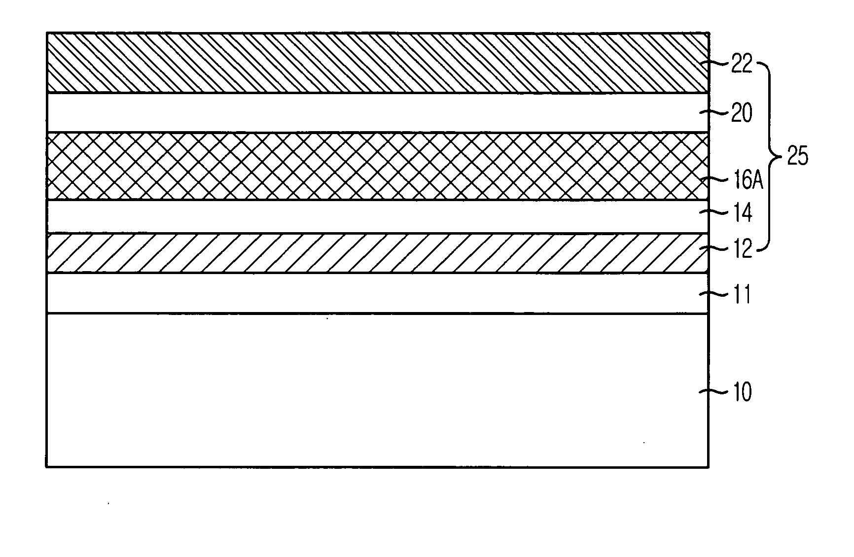
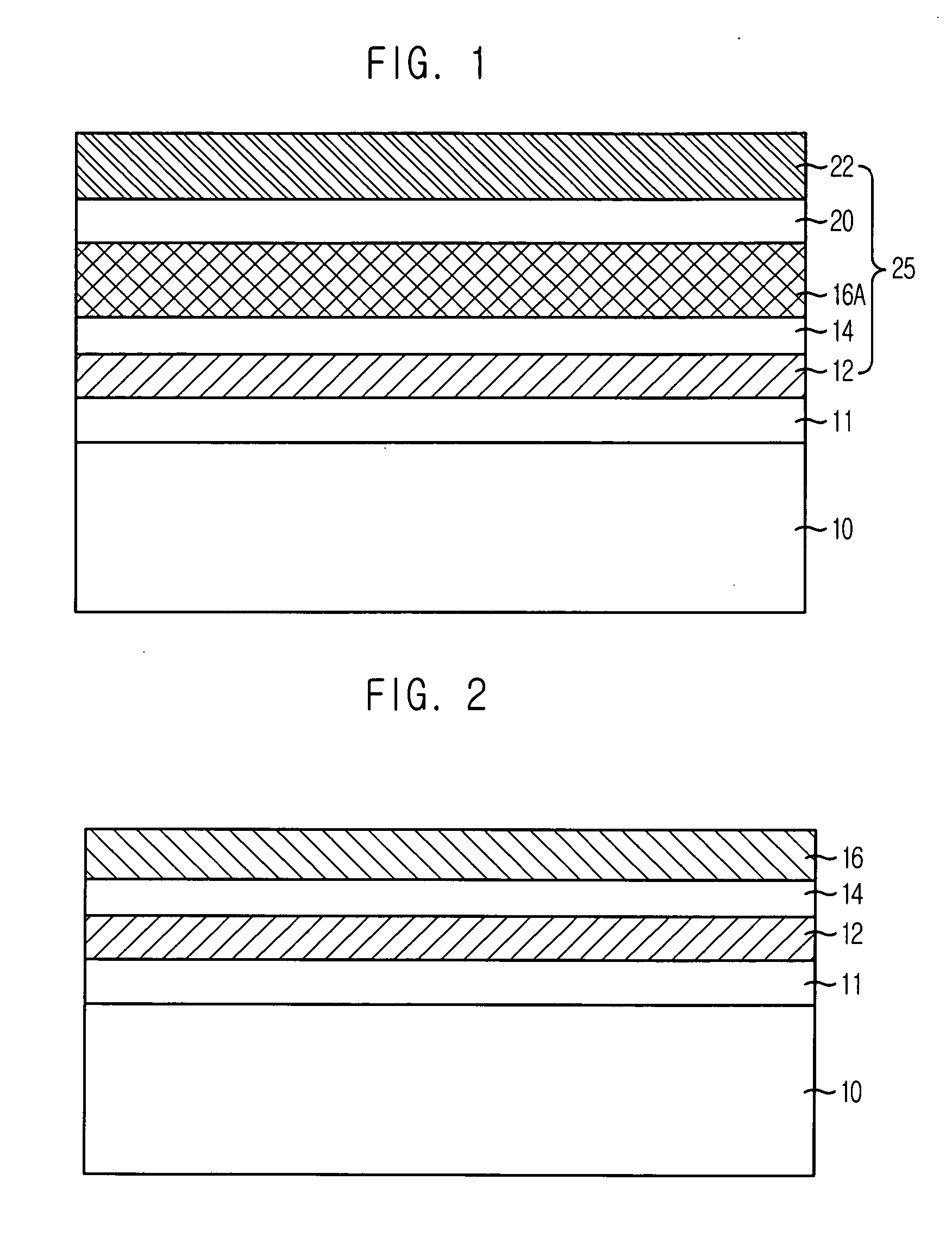
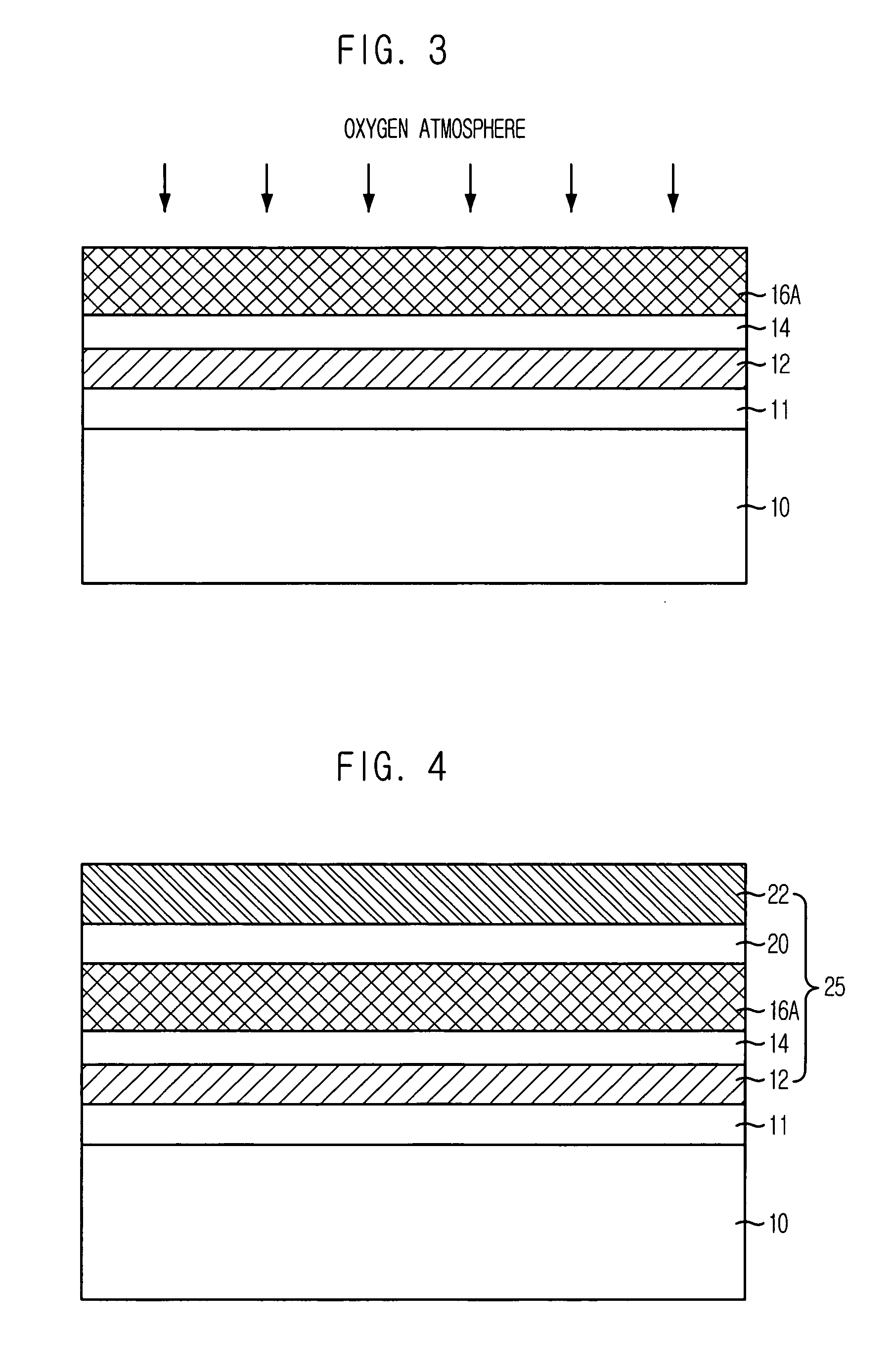
[0024] The dielectric layer in accordance with the first embodiment of the present invention can be applied to a capacitor dielectric layer in a DRAM device. FIG. 1 is a cross-sectional view illustrating the capacitor in the DRAM device formed in accordance with the second embodiment of the present invention, wherein the second embodiment is an example whereto the first embodiment of the present invention is applied.

[0025] Referring to FIG. 1, the capacitor includes: a substrate 10 whereon bit lines are formed, although not illustrated; an inter-layer dielectric (ILD) layer 11 formed on the substrate 10; a bottom electrode 12 formed on the ILD layer 11; a first dielectric layer 16A made of TiO2 in rutile phase formed on the bottom electrode 12; and an upper electrode 22 formed on the first dielectric layer 16A.

[0026] Also, the capacitor in accordance with the second embodiment of the present invention further in...

third embodiment

[0045] Hereinafter, the present invention will be described in detail.

[0046] A dielectric layer in accordance with the specific embodiments of the present invention can be applied to an inter-poly dielectric (IPD) structure or an inter-poly oxide (IPO) structure in a non-volatile memory device. FIG. 5 is a cross-sectional view illustrating a non-volatile memory device formed in accordance with the third embodiment of the present invention, wherein the third embodiment is an example whereto the first embodiment of the present invention is applied.

[0047] Referring to FIG. 5, the non-volatile memory device includes: a gate insulation layer 112 formed on a substrate 110; a floating gate 114 formed on a portion of the gate insulation layer 112; a first dielectric layer 118A made of TiO2 in rutile phase and formed on the floating gate 114; and a control gate 124 formed on the first dielectric layer 118A. The floating gate 114 and the control gate 124 are formed with polysilicon.

[0048] A...


PUM


Abstract

A semiconductor device with a dielectric structure and a method for fabricating the same are provided. A capacitor in the semiconductor device includes: a bottom electrode formed on a substrate; a first dielectric layer made of titanium dioxide (TiO2) in rutile phase and formed on the bottom electrode; and an upper electrode formed on the first dielectric layer.

Description

FIELD OF THE INVENTION [0001] The present invention relates to a semiconductor memory device and a method for fabricating the same; and, more particularly, to a semiconductor device provided with a dielectric layer made of titanium dioxide (TiO2) in rutile phase and a method for fabricating the same. DESCRIPTION OF RELATED ARTS [0002] For a semiconductor memory device, e.g., a DRAM device, the size of a memory cell region for storing 1 bit is becoming smaller as the degree of integration is increasing. Herein, 1 bit is the basic unit for memory information. However, the size of a capacitor cannot be reduced in proportion to the memory cell region reduction. This result is because a dielectric capacity above a certain level is required for each of the unit cells to prevent soft errors and maintain stable operations. Thus, researches for maintaining the capacity of the capacitor within the limited cell region above the certain level is being demanded. Such researches have progressed i...

Claims


Application Information

Patent Timeline
IPC IPC(8): H01L21/8244
CPCH01L29/513H01L29/7881H01L29/66825H10B99/00H10B12/00
Inventor PARK, KI-SEONROH, JAE-SUNG
Owner SK HYNIX INC
Why Eureka
Try Eureka