Scrubber for processing semiconductor waste gas

a technology for processing waste gas and scrubber, which is applied in the direction of synthetic resin layered products, chemical vapor deposition coatings, machines/engines, etc., can solve the problems of large amount of particles, environmental pollution, and harmful to the human body, and achieve the effect of improving the efficiency of burning a semiconductor waste gas

Active Publication Date: 2007-03-08
CLEAN SYST KOREA
View PDF7 Cites 34 Cited by
  • Summary
  • Abstract
  • Description
  • Claims
  • Application Information

AI Technical Summary

Benefits of technology

[0013] Accordingly, the present invention has been made to solve the above-mentioned problems occurring in the prior art, and an object of the prese...

Problems solved by technology

Therefore, if such a reaction gas (hereinafter, to be referred to as “waste gas”) is discharged after use to the atmosphere as it is, it is not only harmful to human body but also causes environmental contamination.
Like this, if such a semiconductor waste gas is burnt, a large quantity of particles is produced.
However, the conventional semiconductor waste gas processing scrubbers as mentioned above have various problems as follows.
First, a conventional scrubber has a problem in that a burner employed in such a scrubber is not superior in efficiency for burning a semiconductor waste gas and thus cannot completely burn the semiconductor waste gas.
That is, there is a problem in that the burner is supplied with fuel and oxygen as well as a semiconductor waste gas, wherein because the waste gas, the fuel and the oxygen are supplied in such a manner as to flow parallel to each other, they are not rapidly mixed with each other, whereby the burner is poor in efficiency for burning the semiconductor waste gas.
Second, the particles, which have been generated after burning the semiconductor waste g...

Method used


Image

  • Scrubber for processing semiconductor waste gas
  • Scrubber for processing semiconductor waste gas
  • Scrubber for processing semiconductor waste gas

Examples


Embodiment Construction

[0081] Hereinafter, a preferred embodiment of the present invention will be described with reference to the accompanying drawings. In the following description and drawings, the same reference numerals are used to designate the same or similar components, so that repeated description on the same or similar components will be omitted.

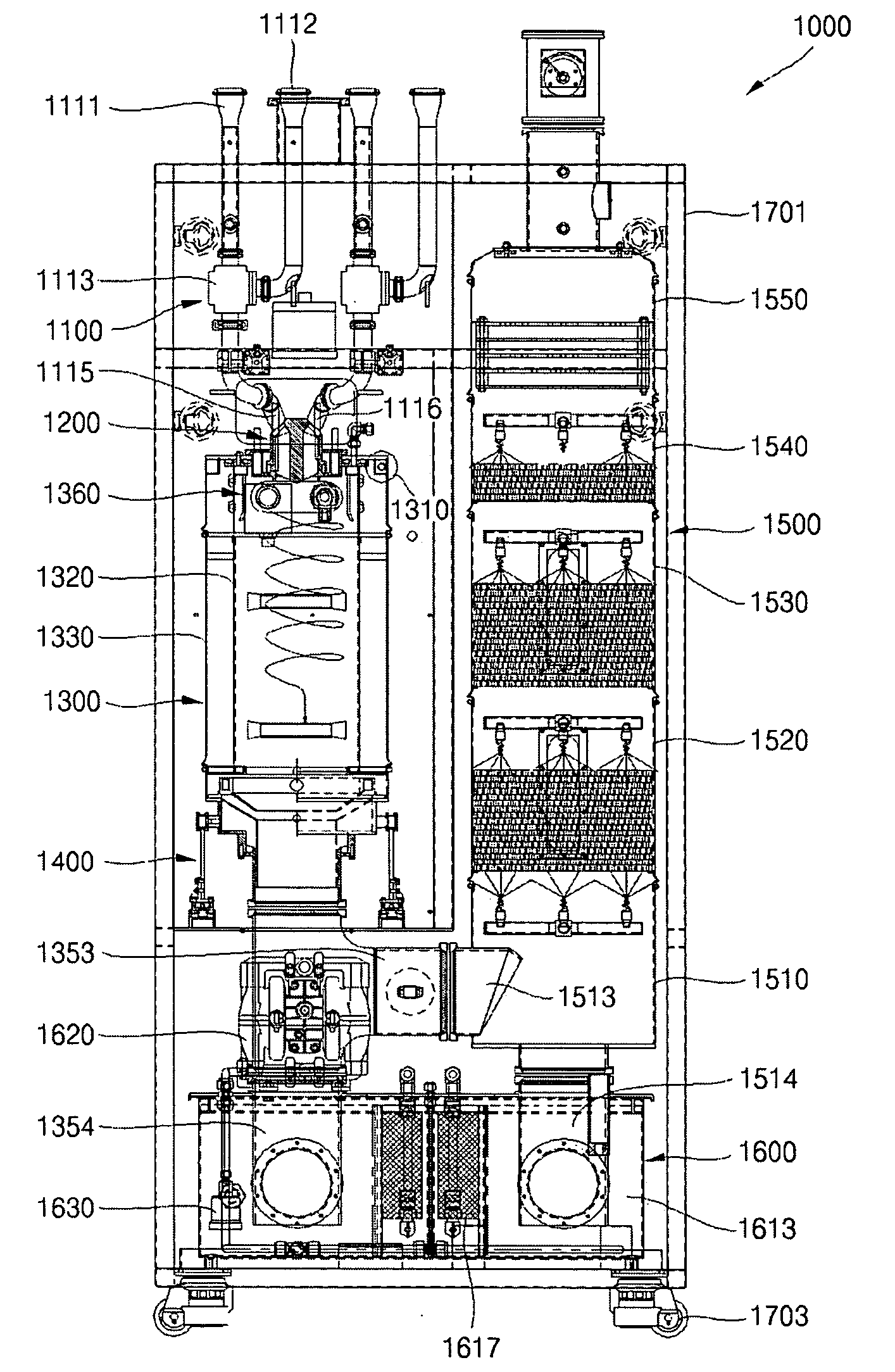
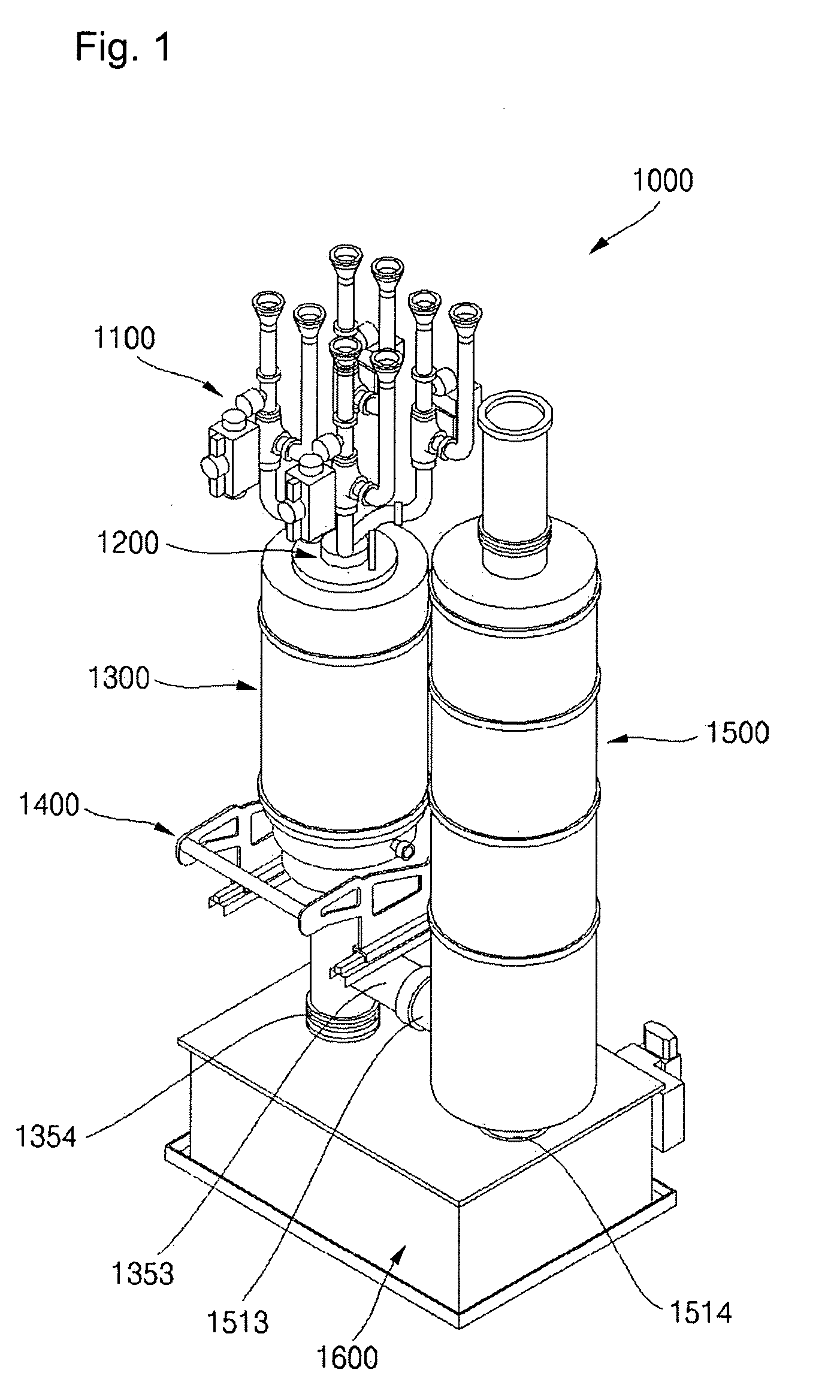
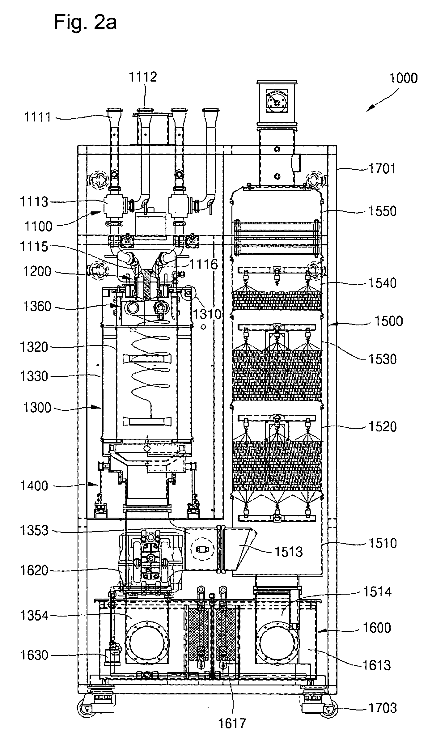
[0082]FIG. 1 is a perspective view showing a main construction of the inventive semiconductor waste gas processing scrubber 1000.

[0083] As shown, the inventive semiconductor waste gas processing scrubber 1000 includes: a supply section 1100 for supplying a semiconductor waste gas, fuel and oxygen, a burner 1200 connected to the supply section 1100 so as to burn the semiconductor waste gas with a flame; a burning chamber 1300 connected to the burner 1200 so as to cause particles or the like, that are produced as the semiconductor waste gas is burnt, to drop; a chamber support section 1400 provided under the burning chamber 1300 so as to support the burn...


PUM

PropertyMeasurementUnit
Angleaaaaaaaaaa
Pressureaaaaaaaaaa
Angleaaaaaaaaaa

Abstract

Disclosed is a scrubber for processing semiconductor waste gas produced in a semiconductor fabricating process, wherein the scrubber burns the waste gas with a flame of a high temperature, filters and captures particles produced after the waste gas is burnt, and discharges particle-filtered waste gas to the atmosphere. The semiconductor waste gas processing scrubber includes: a supply section for supplying semiconductor waste gas, fuel and oxygen; a burner connected to the supply section so as to burn the semiconductor waste gas by flame; a burning chamber joined to the burner so as to cause particles, which are produced as the semiconductor waste gas is burnt, to drop; a wet tower installed at a side of the burning chamber so as to cause the particles, which are transferred from the burning chamber after adsorbing the particles using water, to drop; and a water reservoir tank connected to the burning chamber and the wet tower so as to capture the particles which have dropped from the burning chamber and the wet tower.

Description

CROSS-REFERENCE TO RELATED APPLICATIONS [0001] This application claims priority to and the benefit of Korean Patent Application No. 10-2006-0011011 filed on Feb. 6, 2006, Korean Patent Application No. 10-2006-0011012 filed on Feb. 6, 2006, Korean Patent Application No. 10-2006-0011013 filed on Feb. 6, 2006, Korean Patent Application No. 10-2005-0081838 filed on Sep. 2, 2005 and Korean Patent Application No. 10-2005-0082274 filed on Sep. 5, 2005, in the Korean Intellectual Property Office, the entire contents of which are incorporated herein by references. FIELD OF THE INVENTION [0002] The present invention relates to a scrubber for processing waste gas from a semiconductor process (hereinafter, to be referred to as “semiconductor waste gas processing scrubber”), and in particular to a semiconductor waste gas processing scrubber, which burns the waste gas from a semiconductor process using flame of high temperature, filters and captures the burnt waste gas using water, and then disch...

Claims


Application Information

Patent Timeline
IPC IPC(8): B01D53/34B01D50/00B32B27/02
CPCB01D47/06B01D47/14B01D2258/0216Y02C20/30F23G7/065F23G2209/142F23J2217/50C23C16/4412
Inventor LEE, YOUNG CHANKIM, HYUNG GEUKLEE, SANG KEUN
Owner CLEAN SYST KOREA
Why Eureka
Try Eureka