Semiconductor storage device including electrical fuse module

Inactive Publication Date: 2007-03-15
SOCIONEXT INC
View PDF5 Cites 8 Cited by
  • Summary
  • Abstract
  • Description
  • Claims
  • Application Information

AI Technical Summary

Benefits of technology

[0010] According to this configuration, the fuse elements are melted one by one using the program enable signal transferred by means of the program shift register block, so that the fuse elements can be melted using an existing general-purpose tester without a special tester. Further, since the pr

Problems solved by technology

However, it is difficult for an existing general-purpose tester to supply a current of 10 A according to such programming and pass a current of 10 A concentr

Method used


Image

  • Semiconductor storage device including electrical fuse module
  • Semiconductor storage device including electrical fuse module
  • Semiconductor storage device including electrical fuse module

Examples


embodiment 1

[Embodiment 1]

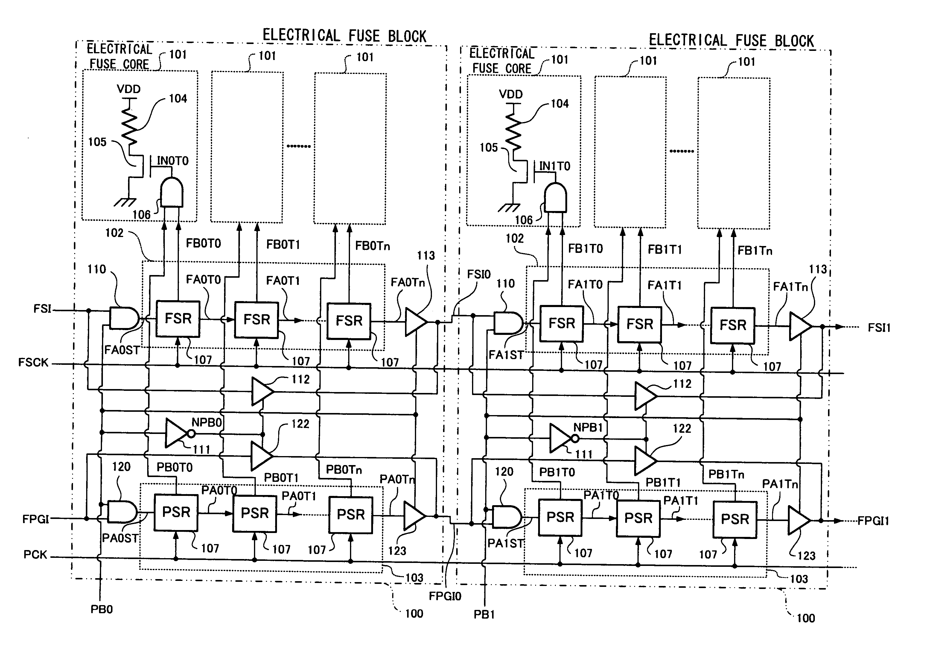
[0056]FIG. 1 is a circuit diagram showing the configuration of a semiconductor storage device including an electrical fuse module according to Embodiment 1 of the present invention. The electrical fuse module includes a plurality of fuse elements.

[0057] In the electrical fuse module of FIG. 1, reference numeral 100 denotes electrical fuse blocks of two or more stages (p stages, the third stage and later are omitted in FIG. 1).

[0058] The stages of the electrical fuse blocks 100 are fed with data clock signal FSCK and program clock signal PCK in a shared manner.

[0059] The initial stage of the electrical fuse block 100 is fed with data signal FSI and program enable signal FPGI and outputs signals FSI0 and FPGI0 which are transferred signals of FSI and FPGI. The second stage and later of the electrical fuse block 100 are fed with FSIm and FPGIm and outputs FSI(m+1) and FPGI(m+1); (m=0 to p−1).

[0060] Each of the electrical fuse blocks 100 is made up of n electrical fuse...

embodiment 2

[Embodiment 2]

[0096]FIG. 3 is a circuit diagram showing the configuration of a semiconductor storage device including an electrical fuse module according to Embodiment 2 of the present invention. The electrical fuse module includes a plurality of fuse elements.

[0097] In the electrical fuse module of FIG. 2, reference numeral 200 denotes electrical fuse blocks of two or more stages (p stages, the third stage and later are omitted in FIG. 2).

[0098] The electrical fuse blocks 200 are fed with data clock signal FSCK and program clock signal PCK in a shared manner. The initial stage of the electrical fuse block 200 is fed with data signal FSI and program enable signal FPGI and outputs signals FA0Tn and PA0Tn which are transferred signals of FSI and FPGI. The second stage and later of the electrical fuse block 200 are fed with FA(m−1)Tn and PA(m−1)Tn and output FAmTn and PAmTn; (m=0 to p−1).

[0099] The electrical fuse block 200 is made up of n electrical fuse cores 101, a data shift reg...

embodiment 3

[Embodiment 3]

[0133]FIG. 6 is a circuit diagram showing the configuration of a semiconductor storage device including an electrical fuse module according to Embodiment 3 of the present invention. The electrical fuse module includes a plurality of fuse elements.

[0134] In the electrical fuse module of FIG. 6, reference numeral 400 denotes electrical fuse blocks of two or more stages (p stages, the third stage and later are omitted).

[0135] The electrical fuse blocks 400 are fed with data clock signal FSCK and program clock signal PCK in a shared manner. The initial stage of the electrical fuse block 400 is fed with data signal FSI and program enable signal FPGI and outputs signals FA0Tn and FPGI0 which are transferred signals of FSI and FPGI. The second stage and later of the electrical fuse block 400 are fed with FA(m−1)Tn and FPGI(m−1) and output FAmTn and FPGIm; (m=1 to p−1).

[0136] In the electrical fuse block 400, the same configurations as those of FIG. 1 are indicated by the s...


PUM


Abstract

Electrical fuse blocks (100) of a plurality of stages are provided each of which includes a plurality of electrical fuse cores (101). The electrical fuse block (100) includes a program shift register block (103) made up of shift registers (107) which are disposed for the respective electrical fuse cores (101), sequentially transmit program enable signal FPGI, and output the program enable signal FPGI to the NMOS transistors (105) of the electrical fuse cores (101). When performing programming according to programming decision signal PBn, the program shift register block (103) transmits the program enable signal FPGI. When not performing programming, the program shift register block (103) skips the program enable signal FPGI.

Description

FIELD OF THE INVENTION [0001] The present invention relates to OTP (One Time Programmable) memory using a semiconductor, and particularly relates to a semiconductor storage device including an electrical fuse module in which fuse elements can be blown and programmed by passage of current. BACKGROUND OF THE INVENTION [0002] Conventionally, electrical fuse modules (electrical fuse devices) are configured using electrical fuse elements made of polysilicon or the like and have been widely used for semiconductor integrated circuits (LSI) for trimming program devices or the like of high-frequency semiconductor devices. In semiconductor integrated circuits including such electrical fuse devices, electrical fuse elements are programmed by passing a large current of about 1 A to melt the fuse elements by means of bipolar transistors. [0003] In recent years, for example, as disclosed in National Publication of International Patent Application No. 11-512879, the following process has been deve...

Claims


Application Information

Patent Timeline
IPC IPC(8): G11C17/00
CPCG11C17/16G11C17/165G11C2229/763G11C29/785G11C29/027
Inventor SUMI, SHINICHIKIKUKAWA, HIROHITOAGATA, YASUHIROSHIRAHAMA, MASANORIKAWASAKI, TOSHIAKINISHIHARA, RYUJIYAMAMOTO, YASUE
Owner SOCIONEXT INC
Why Eureka
Try Eureka