Method of controlling impurity doping and impurity doping apparatus

Inactive Publication Date: 2007-03-15
PANASONIC CORP
View PDF3 Cites 35 Cited by
  • Summary
  • Abstract
  • Description
  • Claims
  • Application Information

AI Technical Summary

Benefits of technology

[0023] With the structure above, dopant can be applied with high accuracy to a predetermined section including a shallow-junction region of the semiconductor device. This allows a semiconductor device to have minimized variations in quality.
[0024] According to the method and apparatus of the present invention, the dose amount of dopant can be controlled with higher accuracy than before. The accurate doping control can extend coping range on semiconductor devices that have been thought to have difficulties in processi

Problems solved by technology

Generally, such a state is very active and therefore easily causes reaction.
The conventional dose-amount control above, however, has a pending problem in the plasma-doping process on a semiconductor device where precise control of the dose amount is required.
Due to variations or errors in the dose amount, variations in semiconductor characteristics cannot be reduced.
That is, the conventional methods have

Method used


Image

  • Method of controlling impurity doping and impurity doping apparatus
  • Method of controlling impurity doping and impurity doping apparatus
  • Method of controlling impurity doping and impurity doping apparatus

Examples


first exemplary embodiment

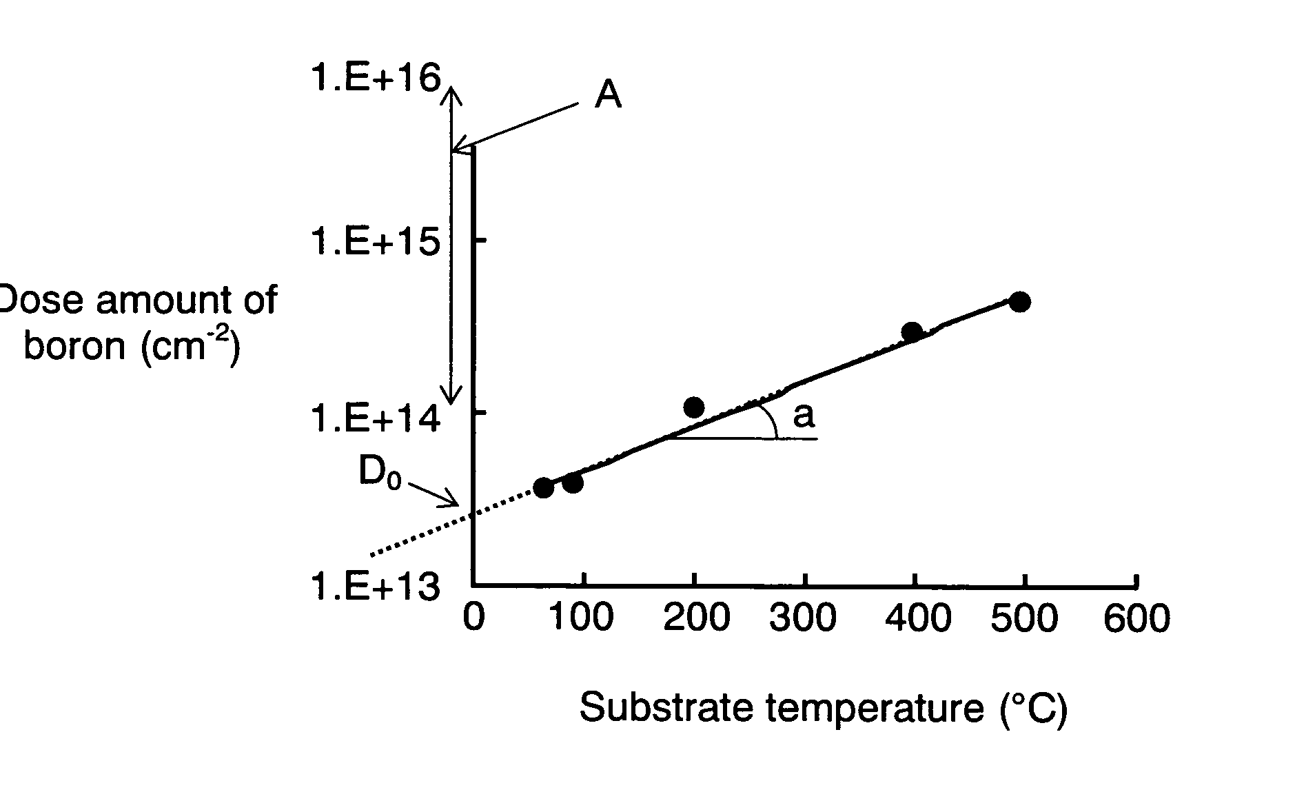
[0049] The description given in the embodiment is about results of gas-doping in which boron was doped into a silicon substrate. In the experiment, a silicon substrate disposed in a chamber underwent helium (He)-plasma irradiation for 20 seconds. Following the completion of the He-plasma irradiation, diborrane (B2H6) gas, which was diluted with helium (He) to have concentration of 5%, was fed into the chamber for 7 seconds with pressure of 1 Pa. While the B2H6 gas was being fed, the surface temperature of the substrate was increased from 60° C. to 500° C. According to the gas-doping through the process above, the relationship between the dose amount of boron and the substrate temperature is similar to that shown in FIG. 1. The relationship between the dose amount of boron (Dgas) and the substrate temperature (T) is expressed by equation (1):

5 Dgas=D0·exp(a·T)   (1),

[0050] where, Dgas represents the dose amount (cm−2) of boron; D0 represents the dose amount (cm−2) of boron at the s...

second exemplary embodiment

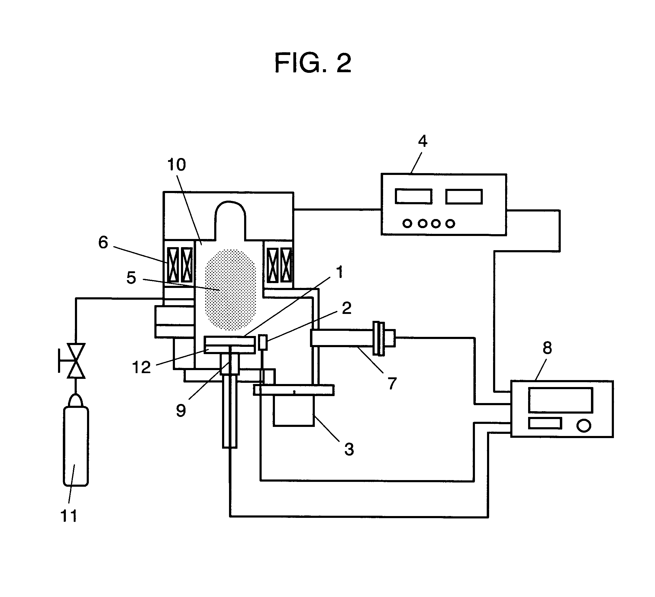
[0057] The description given in the embodiment is about results of plasma-doping in which a dose amount of boron of 3.5×1014 cm−2 was doped into a silicon substrate. In the experiment, a silicon substrate disposed in a chamber underwent diborrane (B2H6)-plasma irradiation for 7 seconds. In the plasma irradiation, the B2H6-gas, which was diluted with helium (He) to have concentration of 0.025%, was fed into the chamber with pressure of 0.9 Pa. While the B2H6-gas was being fed, a bias voltage of 100V—biased by 600 kHz-high frequency power supply—was applied to the silicon substrate. The source power was set at 1500 W The surface temperature of the substrate was kept at 0° C.

[0058] In this case, an amount of B2H6-gas, which is estimated by gas analyzer 7 under a substrate temperature of 0° C., measures 3×1013 cm−2. According to Faraday cup as ion analyzer 2, the estimated dose amount measures 3.2×1014 cm−2. On the other hand, the SIMS (Secondary Ion Mass Spectrometry) measurement afte...

third exemplary embodiment

[0061] In the third embodiment, like the previous embodiment, boron is doped into a silicon substrate by plasma-doping. The target dose amount is 3.5×1014 cm−2. In the experiment, a silicon substrate disposed in a chamber underwent diborrane (B2H6)-plasma irradiation for 60 seconds. In the plasma irradiation, the B2H6-gas, which was diluted with helium (He) to have concentration of 0.025%, was fed into the chamber with pressure of 0.9 Pa. While the B2H6-gas was being fed, a bias voltage of 100V—biased by 600 kHz-high frequency power supply—was applied to the silicon substrate. The source power was set at 1500 W. The surface temperature of the substrate was kept at 0° C. The doping conditions of the embodiment are the same as those of the second embodiment, except for the plasma-irradiating time.

[0062] In this case, an amount of B2H6-gas, which is estimated by gas analyzer 7 under a substrate temperature of 0° C., measures 3×1013 cm−2. The dose amount by gas is, as described above, ...


PUM


Abstract

Disclosed here is a method of controlling a dose amount of dopant to be doped into object (1) to be processed in plasma doping. According to the method, the doping control is formed of the following processes: determining the temperature of object (1), the amount of ions having dopant in plasma that collide with object (1), and types of gases in plasma during doping; calculating a dose amount by neutral gas according to the temperature of object (1), and a dose amount by ions from the determined amount of ions containing dopant that collide with object (1); and carrying out doping so that the sum of the dose amount by neutral gas and the dose amount by ions equal to a predetermined dose amount.

Description

TECHNICAL FIELD [0001] The present invention relates to a method of controlling plasma doping employed in manufacturing a semiconductor, an LCD panel, and the like, and also relates to an impurity doping apparatus. BACKGROUND ART [0002] Conventionally, ion implantation has been widely used as a method of doping impurities used in manufacturing a semiconductor device. As a recent promising technology, attention is now focused on plasma-doping suitable for forming a shallow junction. Plasma-doping is a technique in which a surface of an object to be processed, for example, a semiconductor substrate, undergoes irradiation of plasma containing impurities, i.e., dopant so that dopant is doped therein. [0003] In ion implantation, through a mass segregation process, an ion to be doped is extracted from plasma containing dopant and accelerated before being doped into an object to be processed. On the other hand, in plasma-doping, an object to be processed undergoes direct irradiation of pla...

Claims


Application Information

Patent Timeline
IPC IPC(8): H01L21/66H01L21/26H01L21/04H01L21/00H01L21/265
CPCH01L21/265
Inventor SASAKI, YUICHIRONAKAYAMA, ICHIROOKUMURA, TOMOHIROMAESHIMA, SATOSHI
Owner PANASONIC CORP
Why Eureka
Try Eureka