Controlled depth etched vias

a control depth and via technology, applied in the direction of printed circuits, printed circuit details, printed circuits, etc., can solve the problems of time-consuming and expensive controlled depth drilling or mechanical milling, parasitic signal loss reduction, etc., to minimize parasitic signal loss, minimize process steps, and reduce parasitic signal loss

Inactive Publication Date: 2007-03-22
LITTON SYST INC
View PDF13 Cites 13 Cited by
  • Summary
  • Abstract
  • Description
  • Claims
  • Application Information

AI Technical Summary

Benefits of technology

[0010] The present invention is a printed circuit board processing technique that allows electrical isolation of select vias from either side of printed circuit board. The disclosed process is usable in buried, blind or finished vias. The present invention is realized through a sequence of controlling photo-tools and subsequent etching on feed-through vias. The present method keeps plating from the product surface on one side allowing for standard etching techniques to remove copper connecting via to surface. The present invention also allows tuning of vias through depth etching. Chemical etching is insensitive to printed circuit board thickness variations resulting in consistent depths of removed portion of via. This decreases parasitic signal loss due to material / design considerations.
[0011] Optimization of signal integrity requires tight control of the portion of the through via being removed. Using milling or controlled depth drilling the amount of via removed is dependent on z-axis variations in the printed circuit board. Additionally controlled depth drilling or mechanical milling is time consuming and expensive. Control depth etching allows for the creation of tuned vias from both sides of a panel at the same time. Depth control is achieved chemically. This process permits more complex product through the ability of disconnecting selectively from either side of the product.
[0012] The present invention minimizes repetition of process steps and allows for manufacturing of product using controllable processes. The present invention results in a product that is tuned to minimize parasitic signal loss without having to know material thickness variation.

Problems solved by technology

This decreases parasitic signal loss due to material / design considerations.
Additionally controlled depth drilling or mechanical milling is time consuming and expensive.

Method used


Image

  • Controlled depth etched vias
  • Controlled depth etched vias
  • Controlled depth etched vias

Examples


Embodiment Construction

[0017] So that the manner in which the above recited features, advantages and objects of the present invention are attained can be understood in detail, more particular description of the invention, briefly summarized above, may be had by reference to the embodiment thereof that is illustrated in the appended drawings. In all the drawings, identical numbers represent the same elements.

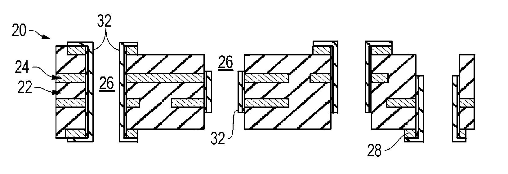
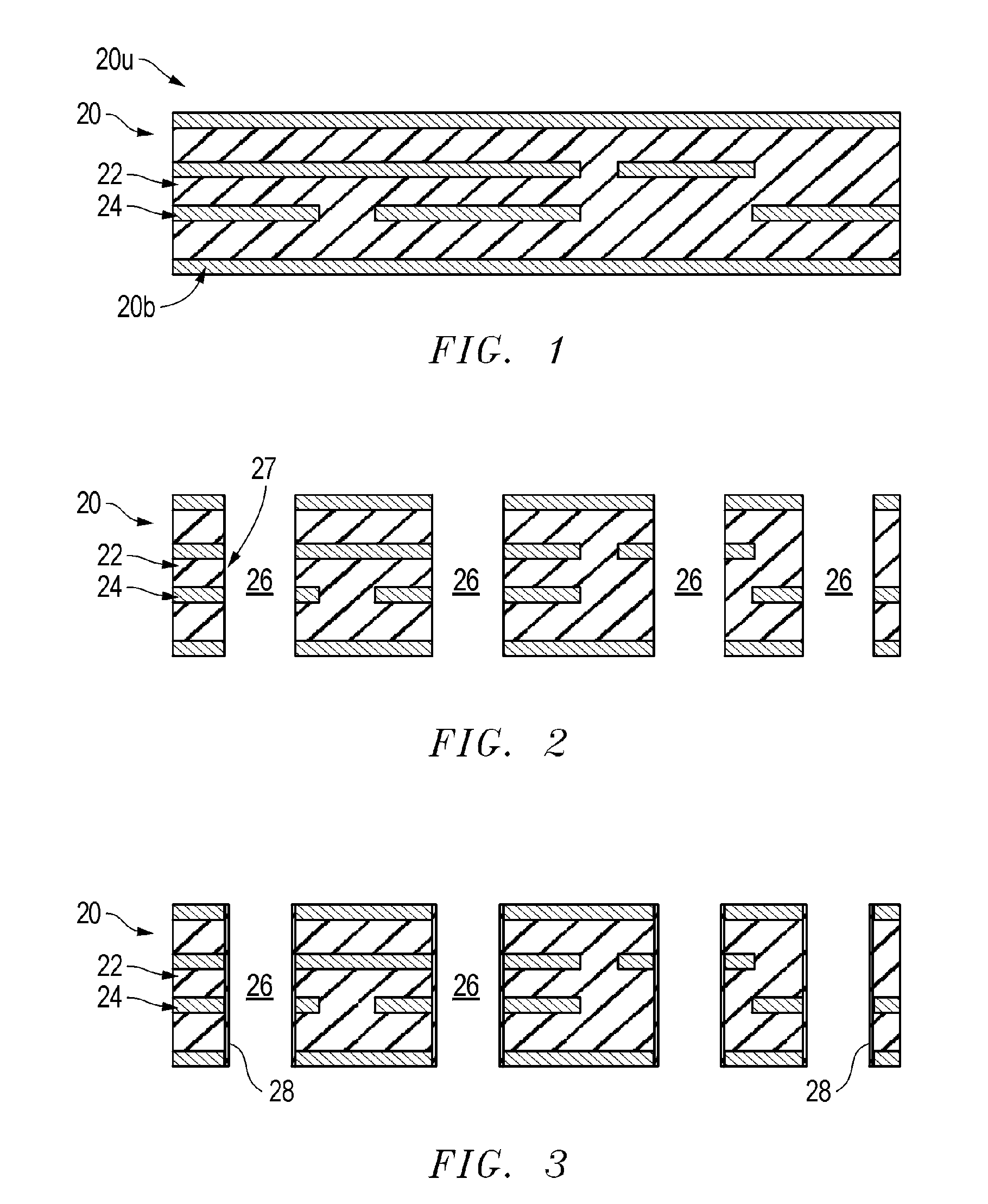
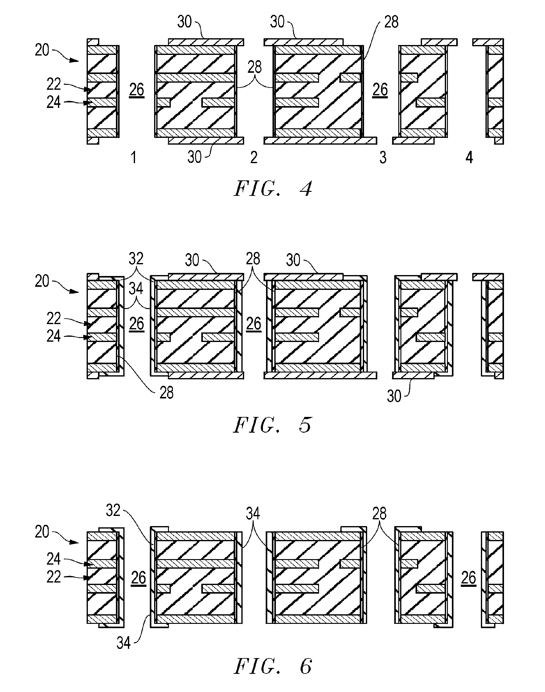
[0018] For illustrative purposes a simple four-layer printed circuit board (PCB) type product 20 will be described. The disclosed method can be used for multiple layers of PCB product 20. For example the four-layer product 20 may be a subset or sub-lamination of a thicker PCB.

[0019] 1. Generally, the desired layers of dielectric material 22, a conductive material 24, such as copper, or other desired component materials or layers are laminated together using a known technique to form the base for the product 20 having an upper surface 20u and a lower surface 20b. Note that this could be a sub-laminati...


PUM


Abstract

A printed circuit board (20) includes a sub-assembly having dielectric (22) and conductive layers (24). A hole (26) extends into the sub-assembly. Metal plating (32) is applied on a barrel (27) of the hole (26). A conductive layer (32) and an etch resist (34) are applied to a first photoresist (30) on the hole barrel (27). The first photoresist (30) is removed and a second photoresist (36) is applied leaving areas to be controlled depth etched exposed. The exposed areas (38) are chemically etched. The second layer of photoresist (36) is removed and a second chemical etch operation is performed to define previously plated features (40) on the sub-assembly (20). The etch resist (34) is then removed.

Description

CROSS REFERENCE TO RELATED APPLICATIONS [0001] This application claims the benefit of U.S. Provisional Application Ser. No. 60 / 595,981, filed Aug. 22, 2005, entitled CONTROLLED DEPTH ETCHED VIAS.BACKGROUND OF THE INVENTION [0002] 1. Technical Field [0003] The invention relates to the field of wiring boards for electronic devices, and more particularly to methods for electrical isolation of vias from either side of a printed circuit board. [0004] 2. Background Art [0005] Electrical isolation of electronic components forming a part of printed circuit boards (PCBs) may be achieved using selected vias or conduits formed in the printed circuit board during the design and manufacture of the printed circuit board. [0006] A prior method, which could be used to solve this problem, is known in the industry as sequential lamination and controlled depth drilling or milling. Sequential lamination is a process whereby a partial group of layers is processed through the normal multilayer lamination...

Claims


Application Information

Patent Timeline
Patent Type & Authority Applications(United States)
IPC IPC(8): H05K1/11
CPCH05K1/115H05K3/062H05K3/064H05K3/427H05K2203/1476H05K2201/09645H05K2203/1184H05K2203/1394H05K3/429
Inventor MURRY, THOMAS D.
Owner LITTON SYST INC
Why Eureka
Try Eureka