

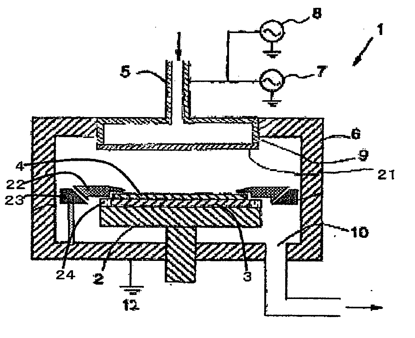
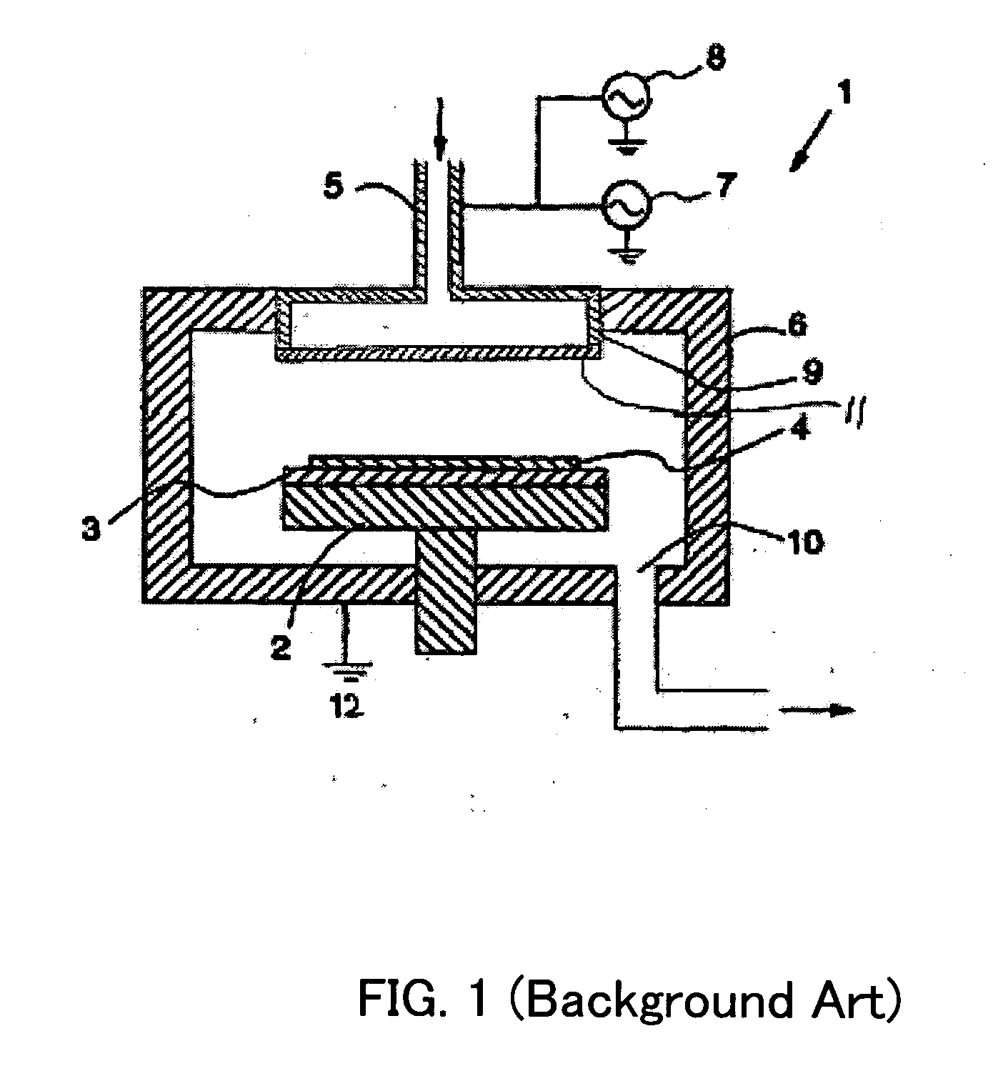
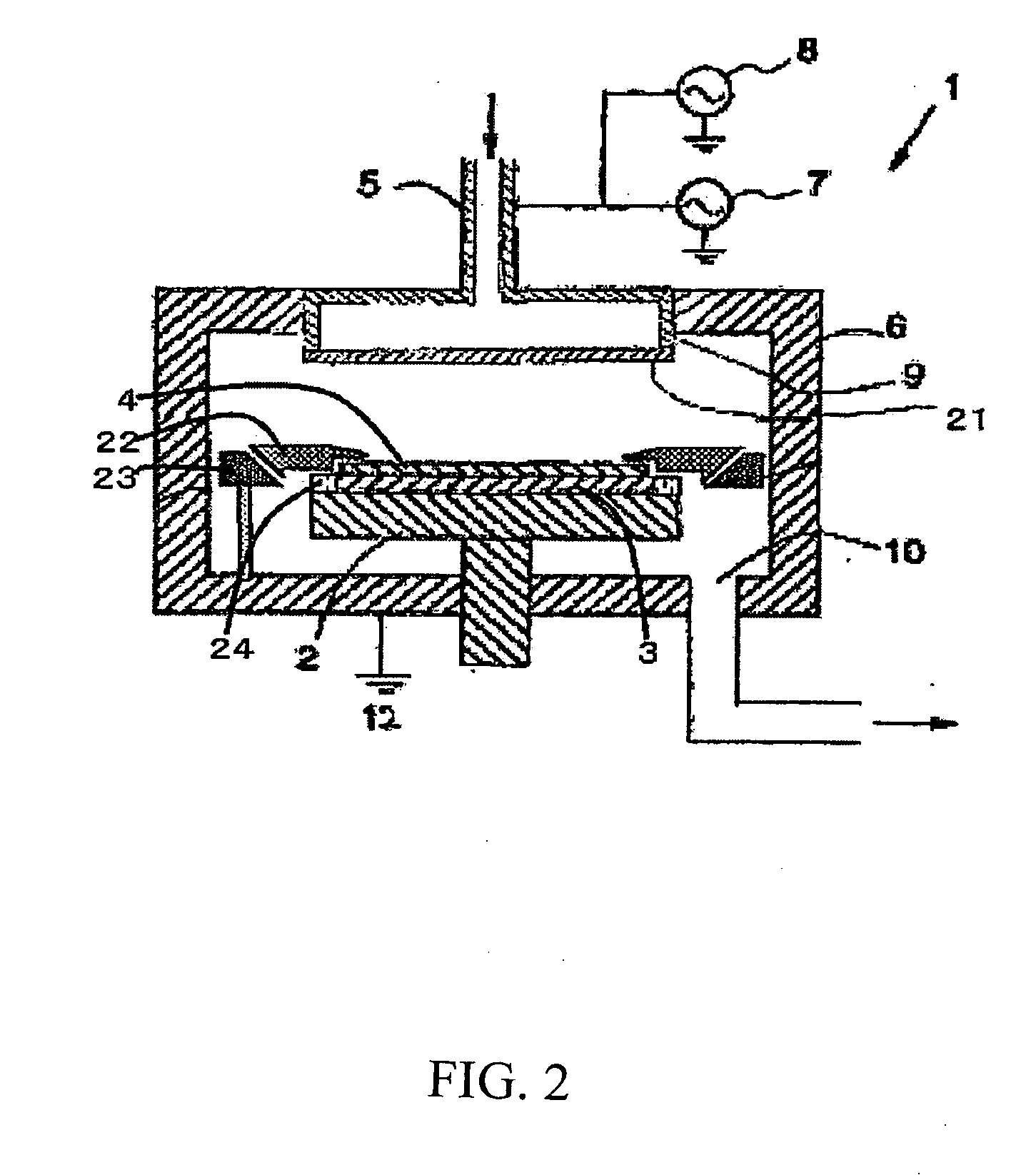
Plasma CVD film formation apparatus provided with mask
a technology of plasma and film, applied in the direction of plasma technique, chemical vapor deposition coating, coating, etc., can solve the problem of poor uniformity of film thickness, and achieve the effect of uniform film thickness and uniform film characteristics
- Summary
- Abstract
- Description
- Claims
- Application Information
AI Technical Summary
Benefits of technology
Problems solved by technology
Method used
Image

Examples
example 1
Mask Material: Alumina, Silicon
[0102] Protrusion area: φ250 mm (Gas inlet hole area: φ205 mm)
[0103] Top plate outer periphery (alumina): Flat
[0104] Clearance between mask and top wafer surface: 0.075 mm
[0105] Film thickness profiles are shown in FIG. 3. It is seen that in the case of an alumina mask as compared with a Si mask, a film thickness is rapidly increased in the vicinity of the outermost periphery by approximately 15% as compared with the center.
example 2
Top Plate Outer Periphery (Alumina): Flat, Trench
[0107] Protrusion area: φ250 mm (Gas inlet hole area: φ205 mm)
[0108] Clearance between mask and top wafer surface: 0.075 mm
[0109] Film thickness profiles are shown in FIG. 4. As compared with a flat type, in the case of a trench type, thickening of a film in an outer periphery is decreased from 25% to 15%. This appears to be a result of widening an effective electrode distance in a wafer outer periphery by placing a wafer on a dielectric material and a gap.
example 3
Clearance Between Mask and Top Wafer Surface: 0.075 mm, 0325 mm, 0575 mm, 0.775 mm
[0110] Protrusion area: φ250 mm (Gas inlet hole area: φ205 mm)
[0111] Mask material: Alumina
[0112] Top plate outer periphery (alumina): Trench
[0113] Film thickness profiles are shown in FIG. 5. Up to a clearance of 0.075-0.575 mm, film formation on a top surface peripheral portion and a side surface portion of a wafer was not observed. However, with a clearance of 0.775 mm, abnormal discharge occurred occasionally; it was judged that film formation was not acceptable. From this result, it can be seen that film formation was satisfactory when a clearance between the mask and the top wafer surface was approximately 0.05-0.7 mm.
PUM
| Property | Measurement | Unit |
|---|---|---|
| Length | aaaaa | aaaaa |
| Length | aaaaa | aaaaa |
| Length | aaaaa | aaaaa |
Abstract
Description
Claims
Application Information