Recursive spacer defined patterning

a spacer and patterning technology, applied in the field of rec, can solve the problems of increasing the difficulty of short-channel effect, high demands on processing engineers, and non-planarity of mugfet, and achieve the effect of improving performance and increasing fin density

Inactive Publication Date: 2007-03-22
DEGROOTE BART +1
View PDF1 Cites 57 Cited by
  • Summary
  • Abstract
  • Description
  • Claims
  • Application Information

AI Technical Summary

Benefits of technology

[0008] A method that further increases the fin density by keeping the fin distance as small as possible is desirable to obtain finFET devices with better performance.

Problems solved by technology

As the scaling of transistor dimensions in planar devices continues, short-channel effects become more of an issue.
The MuGFET's non-planarity however puts high demands on processing engineers and lithographers who have to deal with specific etching, implantation and patterning issues, as well as difficulties in tuning the threshold voltage.
However, most of the time multiple-fin devices are used with several fins contacting large source / drain blocks to improve current drivability.

Method used


Image

  • Recursive spacer defined patterning
  • Recursive spacer defined patterning
  • Recursive spacer defined patterning

Examples


example 1

Fin Quadrupling Processing

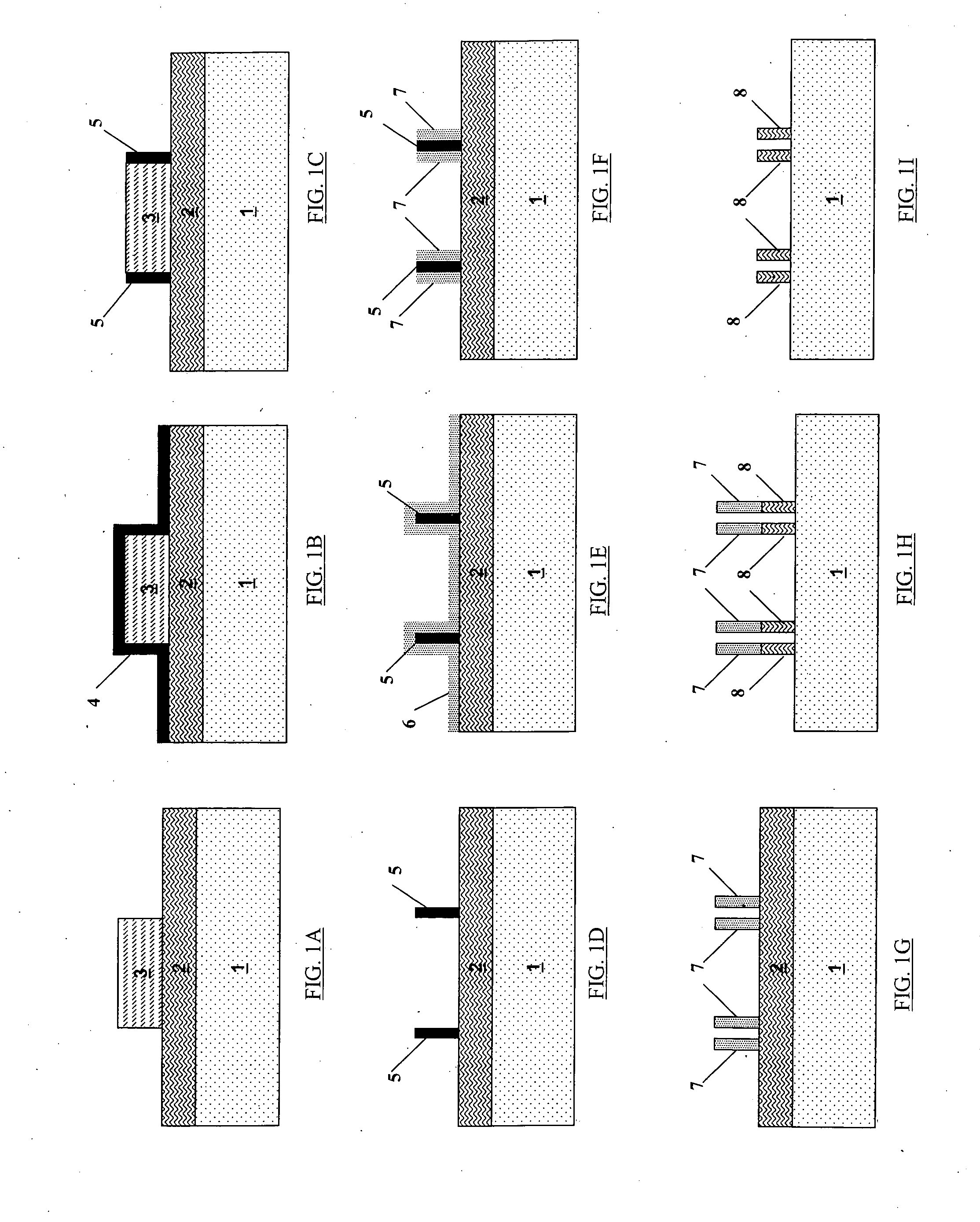
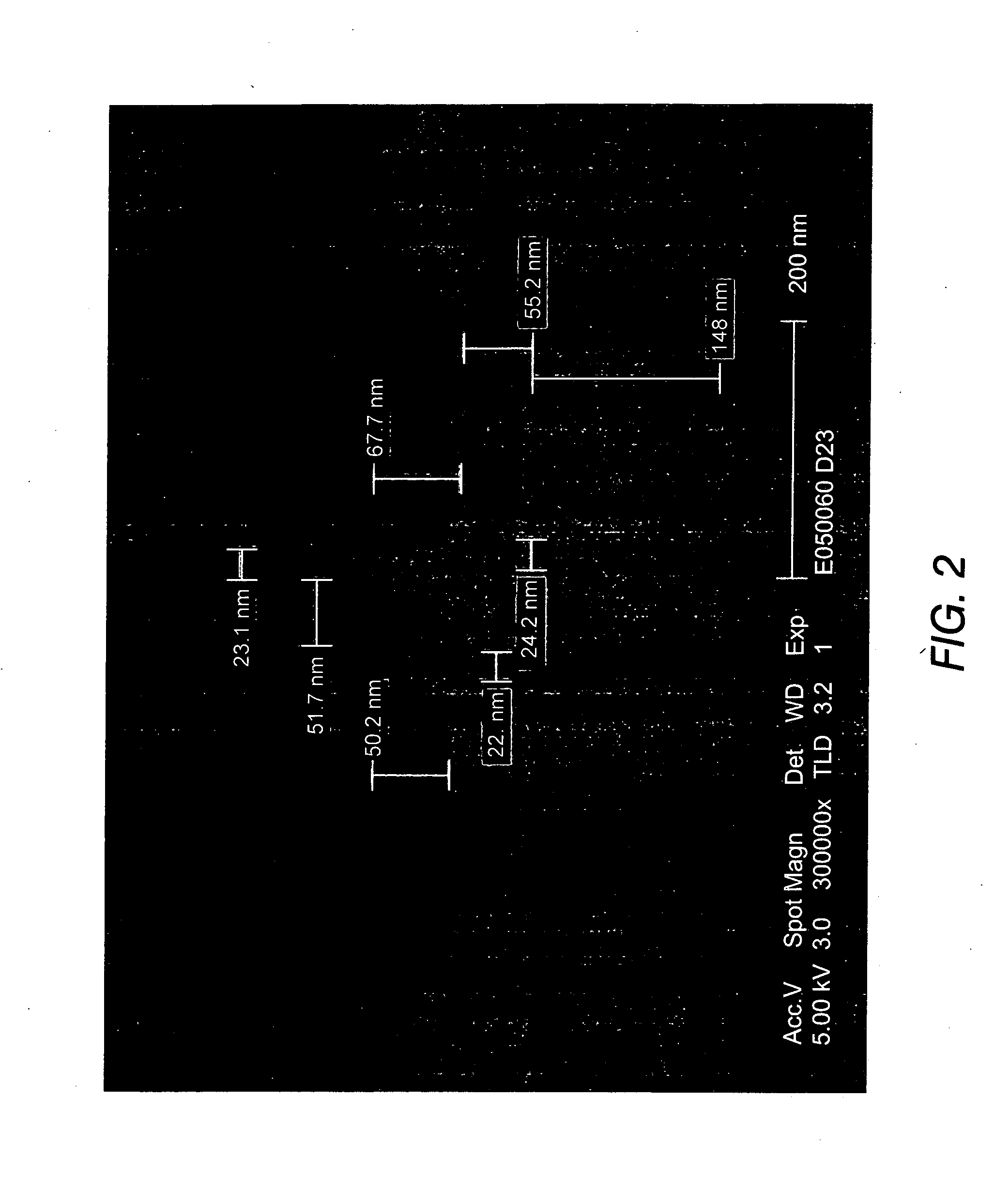
[0155] The experiment starts from a stack comprising the following layers: 65 nm Si / 60 nm TEOS-oxide / 77 nm BARC / 230 nm resist (193 nm). The different process steps are illustrated in FIGS. 6A to 6F.

[0156] Optical lithography (193 nm) is used to pattern a sacrificial hardmask (HM), said sacrificial HM (also referred to in this application as a temporary structure) is made of TEOS-oxide. The BARC layer and the sacrificial HM are opened stopping on the SOI layer (see FIG. 6A).

[0157] Subsequently 30 nm of LP-CVD (Low-Pressure Chemical Vapor Deposition) nitride is deposited on top of the pattern defined by the sacrificial hardmask structure. Consequently a spacer is formed on the sidewalls of the sacrificial hardmask structure. After spacer etch, the wafer is exposed subsequently to a sulfuric peroxide mixture and an ammonia peroxide mixture to remove residual etch products.

[0158] In the next process step, the sacrificial HM structure is removed selectively...


PUM


Abstract

A method for the patterning of a plurality of fins in a MugFET device is provided. The method involves depositing at least one temporary pattern using photolithography. Further processing steps include a combination of depositing a conformal layer and spacer defined patterning of the conformal layer such that a very high density of fins can be achieved. The distance between the fins is no longer determined by photolithography, which is only used to define the temporary pattern which is removed in further processing, but instead by the thickness of the conformal layer, with all fins defined by spacers. Additionally an improved line edge roughness is achieved for the fins using the method.

Description

CROSS-REFERENCE TO RELATED APPLICATIONS [0001] This application claims the benefit of U.S. Provisional Application No. 60 / 717,690 filed Sep. 16, 2005, and European Application No. EP 05447285.7 filed on Dec. 19, 2005. Each of the aforementioned applications is incorporated by reference herein in its entirety, and each is hereby expressly made a part of this specification.FIELD OF THE INVENTION [0002] A semiconductor processing method is provided that is of use in patterning of structures within a semiconductor device, and more specifically within multiple gate devices. BACKGROUND OF THE INVENTION [0003] As the scaling of transistor dimensions in planar devices continues, short-channel effects become more of an issue. [0004] MuGFET devices (multi-gate FET) can provide an answer to this problem. Due to their unique 3-D architecture with gates wrapped around a thin silicon fin, they show excellent gate control over the channel. The MuGFET's non-planarity however puts high demands on pr...

Claims


Application Information

Patent Timeline
Patent Type & Authority Applications(United States)
IPC IPC(8): H01L21/8232H01L21/84H01L21/335H01L21/00
CPCH01L21/0337H01L21/0338H01L21/3086H01L29/785H01L21/84H01L29/66795H01L21/3088
Inventor DEGROOTE, BARTROOYACKERS, RITA
Owner DEGROOTE BART
Why Eureka
Try Eureka