Shunt Passivation Method for Amorphous Silicon Thin Film Photovoltaic Modules

a technology of amorphous silicon thin film and photovoltaic modules, which is applied in the direction of sustainable buildings, climate sustainability, semiconductor devices, etc., can solve the problems of high defect density, unacceptably low efficiency of solar cells, and destructive approaches of several folds, and achieve low shunting defects, good output power, and high yield

Inactive Publication Date: 2007-03-29
TERRA SOLAR GLOBAL
View PDF2 Cites 76 Cited by
  • Summary
  • Abstract
  • Description
  • Claims
  • Application Information

AI Technical Summary

Benefits of technology

[0016] In accordance with the present invention, there is provided a design for control of shunt defects in semitransparent hydrogenated amorphous silicon (a-Si:H) based p-i-n type thin film photovoltaic (PV) modules of thin i-layer. By inclusion of a dummy film of a-Si:H based alloy material of good translucence and sufficient electrical resistivity between the p-i-n layers and the back electrode, the PV modules will possess lower electrical shunting defects, improved output power, higher product yield, and better reliability than devices without such a shunt-reducing layer. The said a-Si PV modules will permit adequate light transmission, through all the thin film layers, to be suitable for building integrated applications, such as PV windows or sky lights. The light transmission through the PV module does not rely on selected removal of a-Si films or electrodes. Rather, all the thin films in the PV device are individually transparent to a satisfactory degree. In particular, the present invention allows the use of very thin a-Si:H intrinsic layer (the i-layer) in p-i-n type large area PV modules without suffering performance and yield loss due to electrical shorting through defects or insufficient coverage of a-Si:H i-layer between the electrodes. According to this invention, shunt passivation can be effectively and entirely provided by additional, PV-inactive a-Si:H based thin films produced by the same manufacturing process for various a-Si p, i, n layers used in conventional a-Si:H PV module fabrication, without using foreign or exotic procedures or materials. Specifically, p-i-n-“i”-n type device structure is proposed to replace conventional p-i-n device of thin i-layer prone to shunting defects. In the p-i-n-“i”-n configuration, the “i”-layer situated between two n-layers is a dummy layer that serves to passivate shorting defects through the first i-layer which is the active photo-electric component in the solar cell. The shunt blocking dummy layer may comprise multiple a-Si alloy thin films of high electrical resistance and good optical transmission, inter-connected by more conductive, n-type a-Si:H based thin films.

Problems solved by technology

This is due to the very high density of defects in doped a-Si:H alloy thin films.
Hence, the thickness of a-Si:H alloy i-layer has a lower-limit threshold, below which the solar cell would have unacceptably low efficiency both because of the device physics flaw and because too little light can be converted to electricity, on the ground that i-layer thickness largely determines the amount of light that can be absorbed and gainfully converted to electrical power.
The drawback of this ‘destructive’ approach is several folds: slow and costly laser scribing; non-uniform looking pattern; the transparency being proportional to the loss of PV active area (loss of module power).
Significant damage to module occurs when ‘dot’ pattern is generated by laser pulses used to blow-away a-Si:H film one spot at a time, leading to excessive power loss.
The foremost technical obstacle is shunting through the very thin a-Si:H i-layer film (<350 nm).
Especially for the more transparent windows requiring thinner a-Si:H (e.g., <200 nm), shunting or short-circuit pathways through defects in a-Si:H including pinholes and sharp imperfections in film geometry are largely unavoidable.
Notice that even for a-Si:H PV devices with thick a-Si:H i-layers, shunting is a prevalent problem as discussed in the prior arts cited below.
Again, the problem of shunting through thin a-Si:H i-layer is the biggest roadblock to practical production and economic application of such devices.
The above procedures are elegant and can be very effective, but they are also very elaborate and require sophisticated instrumentation (expensive, high-cost) and a great deal of labor, in addition to the time required that severely limits the throughput for large area PV module production which can have tens of thousands of small defects per square foot of thin film coating.
These wet processes are time consuming and labor-intensive, in addition to its slow processing speed and special equipment requirements.
Also, there is no guarantee that insulating film will not be deposited on non-defective areas of semiconductor thin film.
This method is highly questionable since fine, tiny defects in very thin films (which can be very densely and randomly dispersed over large continuous plates or sheets) are unlikely to selectively respond to bias voltages.
Most of the earlier proposed solutions (prior arts) have shortcomings that are either technically unsound, or impractical in terms of added costs for PV module manufacturing, or aesthetically unappealing for the finished products.
The necessary thinness of a-Si:H i-layer presents a unique challenge that must be dealt with using custom-tailored solutions.
We cannot simply borrow a technique or a combination of techniques stated in prior arts.
Hence, the shunt-reduced BIPV module will not produce higher output power because of lower collection efficiency of photo-generated electric current despite lower shunting.
Furthermore and just as importantly, none of the prior arts describes a simple method of shunt prevention tightly integrated with the deposition of a-Si:H i-layer, without resorting to additional equipment or additional plate handling, during the production of the shunt-reduced a-Si:H PV modules.
The proposed solutions are all too cumbersome and incompatible with traditional a-Si:H PV module manufacturing process flow.
In fact, none of the prior arts deals with the electrical leakage of the p-i-n structure by simply making repeated use of the various layers, especially the i-layers that can be made wider-bandgap and insulating, in reducing or passivating defects associated with the thinness of any individual i-layer.

Method used


Image

  • Shunt Passivation Method for Amorphous Silicon Thin Film Photovoltaic Modules
  • Shunt Passivation Method for Amorphous Silicon Thin Film Photovoltaic Modules
  • Shunt Passivation Method for Amorphous Silicon Thin Film Photovoltaic Modules

Examples


Embodiment Construction

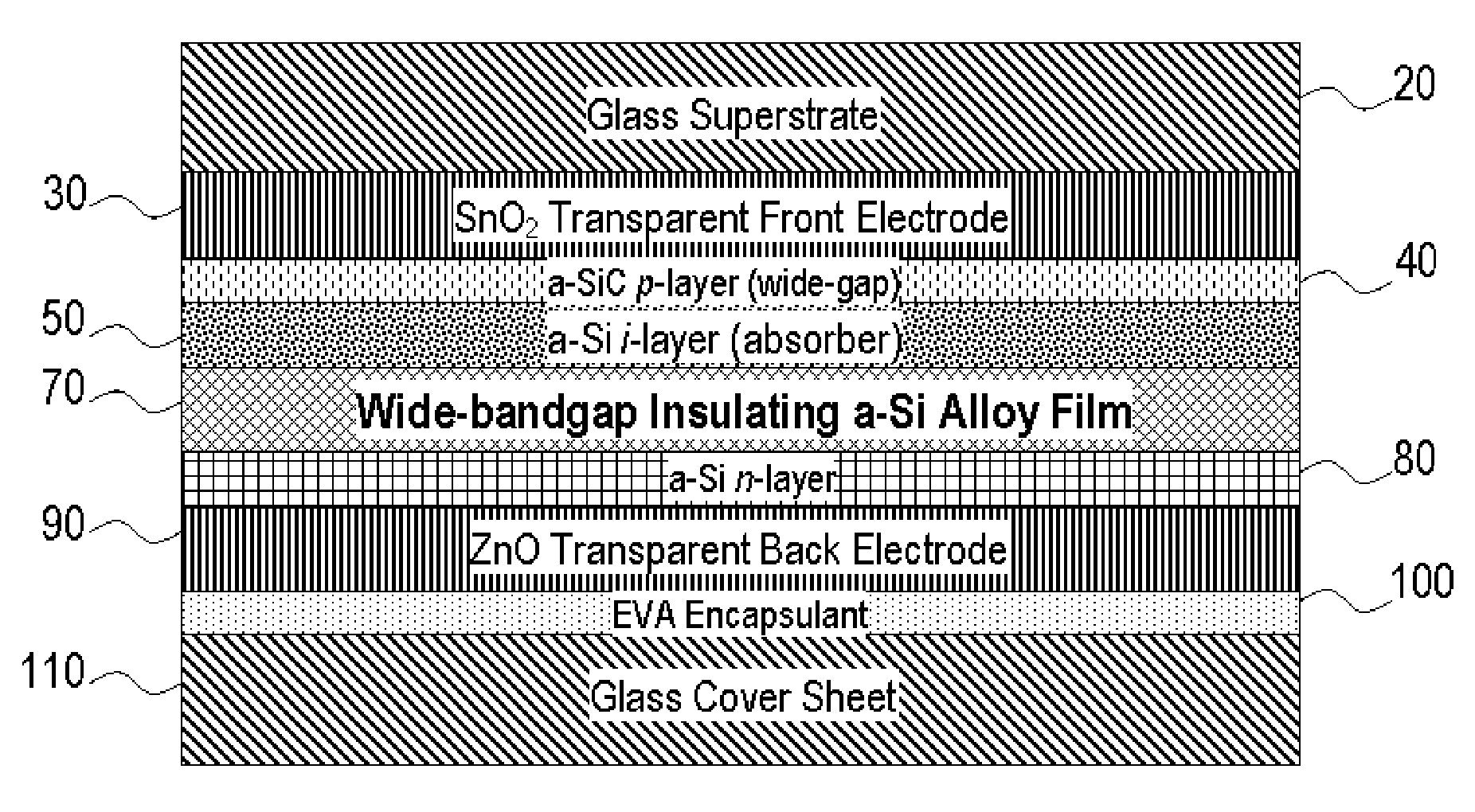
[0020] The present invention entails a simple, lower-cost, robust and effective scheme for negating shunting defects in photovoltaic (PV) modules containing a thin hydrogenated amorphous silicon (a-Si:H) active absorber-converter layer appropriate for semi-transparent or see-through PV applications. FIG. 1 shows the cross section of a standard single junction, p-i-n type solar cell encapsulated between two glass plates. The solar cell includes flat glass substrate 20 (also known as superstrate in this type of device configuration), transparent front electrode 30 (transparent conductive oxide or TCO), a-Si:H alloy p-layer 40, a-Si:H i-layer 50 (intrinsic amorphous silicon), a-Si:H n-layer 80, transparent back electrode 90, lamination agent 100 (encapsulation medium), and glass cover plate 110. Also shown in FIG. 1 is an optional a-Si:H based shunt-reducing layer 70, deposed between a-Si:H i-layer 50 and a-Si:H n-layer 80. Without the wide-bandgap, insulating, a-Si:H based shunt-reduc...


PUM


Abstract

A method for reducing shunt-related defects is described for hydrogenated amorphous silicon (a-Si:H) thin film photovoltaic modules with thin active a-Si:H absorber as required by building integrated photovoltaic windows and sun-roofs with adequate transmission of sunlight. Without shunt-passivation, p-i-n type large area photovoltaic modules with very thin a-Si:H i-layer will suffer excessive performance, yield, and reliability losses due to electrical shorting through i-layer defects. Wide-bandgap a-Si:H based alloy films of sufficient resistivity are deposed between the active solar cell and the conductive back electrode to provide a barrier to leakage current flow. Such a-Si:H based barrier films of high optical transparency are dummy films that do not directly contribute to energy conversion. The shunt-passivation films are entirely produced by the same conventional manufacturing process for a-Si:H photovoltaic devices without invoking complicated or exotic materials or procedures proposed in prior arts.

Description

BACKGROUND OF THE INVENTION [0001] Due to increasing demands for clean, safe, sustainable, and reliable sources of energy, photovoltaic (PV) systems are undergoing rapid expansion in industrial technology development and in the energy marketplace. Hydrogenated amorphous silicon (a-Si:H) thin films, and the related alloys of hydrogenated amorphous silicon with other elements of various optical bandgaps tailored for various amounts of optical absorption for a given amount of material thickness, have become a relative mature family of PV materials for commercial PV module production that offers low-cost, large area capability, good efficiency, and particularly easy integration with building materials such as windows, roofs, and facades. Due to its relatively wide optical bandgap, a-Si:H is especially well suited to making building integrated PV (BIPV) products, for which the transparency of the BIPV can be controlled, among other things, by the thickness of the a-Si:H layers, particula...

Claims


Application Information

Patent Timeline
Patent Type & Authority Applications(United States)
IPC IPC(8): H01L31/00
CPCH01L31/075Y02B10/12H01L31/0468H01L31/0488Y02E10/548Y02A30/60Y02B10/10
Inventor LI, YUAN-MINKISS, ZOLTAN J.
Owner TERRA SOLAR GLOBAL
Why Eureka
Try Eureka