Memory with high dielectric constant antifuses and method for using at low voltage

a memory and dielectric constant technology, applied in the field of nonvolatile memory array programming and reading, can solve the problems of antifuses and diodes made from films of silicon dioxide that have already been made just a few atoms thick, not to be made thinner, etc., to achieve low voltage, short antifuse, and reliable reading and writing

Inactive Publication Date: 2007-03-29
SANDISK TECH LLC
View PDF18 Cites 76 Cited by
  • Summary
  • Abstract
  • Description
  • Claims
  • Application Information

AI Technical Summary

Benefits of technology

[0011] An aspect of the invention is to assure that the dielectric constant of the insulator used for the memory cell antifuse is higher than that of silicon dioxide (3.9). In particular, a dielectric constant range of approximately 5 to 27 in the antifuse and a band gap smaller than that of silicon work well to produce memory cells that can be reliably read and written at lower voltages than memory cells of silicon dioxide and silicon.
[0012] When the antifuse is formed from an insulator having a dielectric constant above about 5 and the diode is a thin film with a band gap smaller than silicon, the memory cells can be programmed by applying a low voltage in a direction opposite that of natural current flow through the diode, which shorts the antifuse to produce the programmed memory cell. A programming voltage sufficient to short the antifuse can be lower than that required to program a memory cell made from a silicon dioxide antifuse and a doped silicon diode. While a selected memory cell is being programmed, unselected memory cells preferably receive minimal voltage, thus minimizing power consumption in the memory array.
[0013] It is also advantageous to program such a memory cell by applying two voltages in the forward direction of the diode. The first application of voltage shorts the antifuse (forms a conductive path through the antifuse), and the second application of voltage makes a larger opening at the location of the short, thus reducing resistance to current flow through the short location.
[0014] It is important to avoid disturbing or programming unselected memory cells while programming the selected cells. It is also important to avoid disturbing any of the memory cells while reading the memory cells, and this is true for the life of the device, which may be on the order of 10 years. A memory cell array is accessed by word lines and bit lines, typically running orthogonal to each other in separate horizontal layers of an integrated circuit structure, such that each memory cell is accessed by one word line and one bit line. The memory cells of the present invention each comprise an antifuse in series with a diode. The antifuse may be placed at either the cathode end or the anode end of the diode. According to one aspect of the invention, while a voltage sufficient to short an antifuse is applied to a bit line contacting the selected memory cell and a ground voltage is applied to a word line contacting the selected memory cell, a voltage less than or equal to the diode threshold voltage is applied to bit lines of unselected cells and a voltage that is lower than the voltage sufficient to short an antifuse of a memory cell by one diode threshold voltage is applied to word lines contacting unselected memory cells. This assures that the selected memory cell is programmed and that unselected memory cells are not programmed or otherwise disturbed.

Problems solved by technology

But antifuses and diodes made from films of silicon dioxide have already been made just a few atoms thick, and can not be made thinner.

Method used


Image

  • Memory with high dielectric constant antifuses and method for using at low voltage
  • Memory with high dielectric constant antifuses and method for using at low voltage
  • Memory with high dielectric constant antifuses and method for using at low voltage

Examples


Embodiment Construction

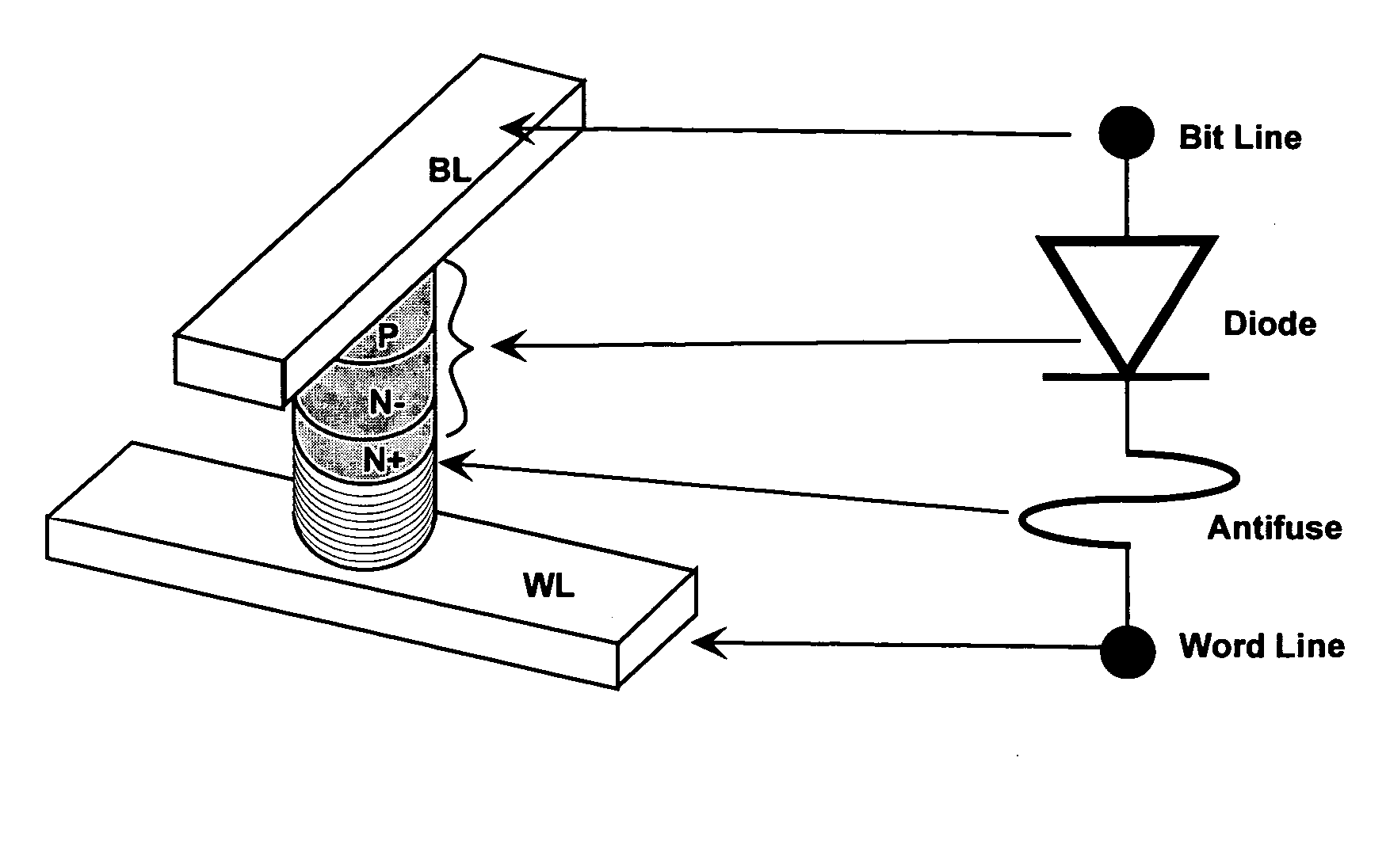
[0026] When developing improvements in integrated circuit memories, it is desirable to reduce the cost of manufacturing while improving operating speed, reducing power consumption, and maintaining a good useful lifetime of the devices. The present invention is directed to memory arrays in which memory cells are formed from a diode and an antifuse connected in series. Preferred embodiments orient the diode and antifuse in a vertical stack between word lines and bit lines.

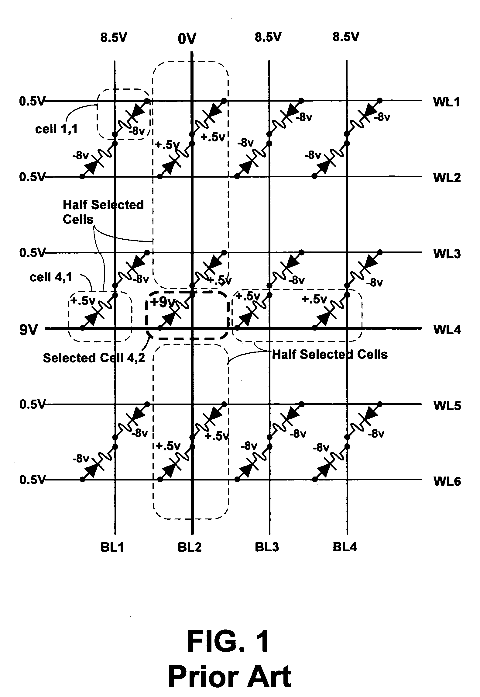
[0027] A critical requirement for shrinking memory devices to deep submicron sizes is to reduce the voltage levels required to write and read the memory cells. For example, whereas the prior art programming voltage illustrated in FIG. 1 is about 9 volts, the present invention will allow programming in the range of 3 to 5 volts. Read voltage can similarly be reduced to about 1 to 1.5 volts. Reducing the required read and write voltages of the memory cells also allows shorter channel length CMOS devices to be used in ...


PUM


Abstract

A memory array having memory cells comprising a diode and an antifuse can be made smaller and programmed at lower voltage by using antifuse materials having higher dielectric constant and higher acceleration factor than silicon dioxide, and by using diodes having lower band gaps than silicon. Such memory arrays can be made to have long operating lifetimes by using the high acceleration factor and lower band gap materials. Antifuse materials having dielectric constants between 5 and 27, for example hafnium silicon oxynitride or hafnium silicon oxide are particularly effective. Diode materials with band gaps lower than silicon, such as germanium or a silicon-germanium alloy are particularly effective.

Description

RELATED APPLICATIONS [0001] This application relates to concurrently filed U.S. application Ser. No. ______ (attorney docket number MA-153) by N. Johan Knall, entitled “REVERSE-BIAS METHOD FOR WRITING MEMORY CELLS IN A MEMORY ARRAY”; and to U.S. application Ser. No. ______, (attorney docket number MA-154) by James M. Cleeves, entitled “MEMORY CELL WITH HIGH-K ANTIFUSE FOR REVERSE BIAS PROGRAMMING”; all filed herewith and incorporated herein by reference.BACKGROUND OF THE INVENTION [0002] The invention relates to programming and reading an array of nonvolatile memory cells each comprising a diode in series with an antifuse. [0003] Integrated circuit memories are typically large arrays of memory cells connected between bit lines and word lines. In order to achieve reliable programming and reading of the memory cells within the array, memory cells selected to be programmed or read must be isolated from memory cells that are not selected. Also, as it becomes increasingly important to mi...

Claims


Application Information

Patent Timeline
Patent Type & Authority Applications(United States)
IPC IPC(8): H01L27/10H01L21/82
CPCG11C17/16H01L23/5252H01L27/101H01L45/12H01L45/04H01L45/146G11C17/00H01L2924/0002H01L2924/00H10N70/801H10N70/20H10N70/8833
Inventor YANG, XIAOYUSCHEUERLEIN, ROY E.LI, FENGMEEKS, ALBERT T.
Owner SANDISK TECH LLC
Why Eureka
Try Eureka