Self-shielded electronic components

a technology of electronic components and shielding, applied in the field of electronic components, can solve the problems of affecting the output power and operating frequency, and affecting the operation of the active device, so as to reduce the energy loss, and increase the magnetic coupling between the first and second conductors

Inactive Publication Date: 2007-03-29
CHEUNG TAK SHUN +1
View PDF6 Cites 36 Cited by
  • Summary
  • Abstract
  • Description
  • Claims
  • Application Information

AI Technical Summary

Benefits of technology

[0016] Advantageously, the low-voltage conductor portion of the electronic component acts to shield the electric field from passing from the higher voltage conductor portion to a lossy surrounding, resulting in reduced energy loss. The portion of the conductor that acts as a shield can also be used for shielding electric field from passing from other conductors to the surroundings. In an alternative embodiment, the low-voltage conductor shields a second, higher-voltage conductor thereby reducing energy lost to the surroundings. Also, in the transformer according to an aspect of the present invention, magnetic coupling between the first and second conductors is increased as magnetic flux leakage is reduced, thereby decreasing signal attenuation. Further, efficiency of the electronic component is increased as current crowding causes the current to flow on edges of the first conductor that are closest to the second conductor. Because the first conductors are at least partially surrounded by the second conductors, current crowding causes the current to flow on all edges proximal the second conductors thereby increasing the surface area over which current flows and decreasing the Ohmic loss.

Problems solved by technology

Implementation of a 24 GHz power amplifier in silicon technology, for example, is hindered by transmission line effects that change the behavior of the signals being processed considerably.
In addition, gain-bandwidth and breakdown voltage limitations of active devices constrain both the output power and operating frequency.
Thus, implementation of such an amplifier is limited to more expensive substrate materials than silicon IC technology.
Such materials cause the final product to be priced out of range for many consumer electronic applications.
However, such balun power combiners suffer several disadvantages.
This is caused by leakage of the magnetic flux produced by alternating current flowing in either conductor, which results in signal loss and attenuation.
Current crowding due to skin effect increases with increasing frequency, and results in Ohmic loss and attenuation of the RF signal.
This energy loss attenuates the desired RF signal and reduces the efficiency of electronic circuits employing the inductor.
Such electronic components suffer disadvantages, however.
Further, other circuitry components are added in series, thereby introducing parasitic elements in series.
Clearly the prior art electronic components suffer significant loss from the conductor (or portions thereof) to the lossy substrate, thereby reducing efficiency and performance.

Method used


Image

  • Self-shielded electronic components
  • Self-shielded electronic components
  • Self-shielded electronic components

Examples


Embodiment Construction

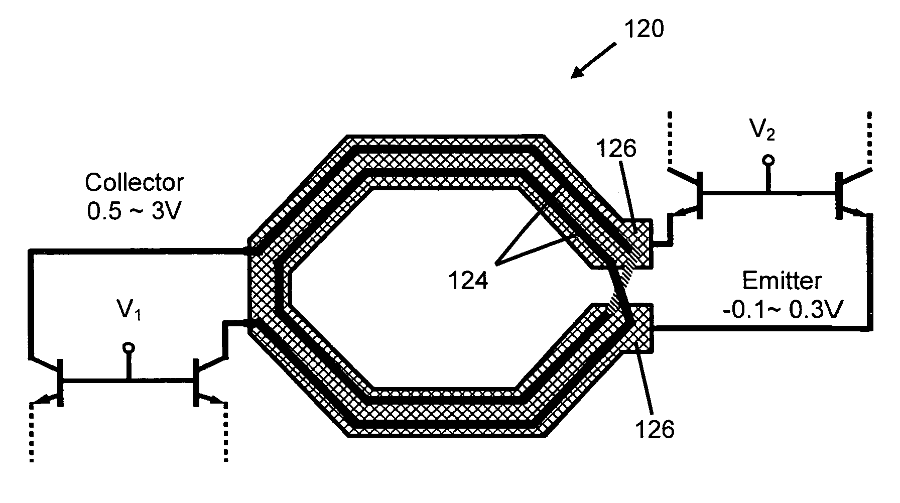
[0031] Reference is made to FIG. 4 to describe an electronic component 120 according to one embodiment of the present invention. The electronic component includes at least one first conductor 124 for operating at a first voltage applied thereto and at least one second conductor 126 for operating at a second voltage applied thereto. The second voltage is smaller than the first voltage and at least a portion of the second conductor 126 is located on at least one side of the first conductor 124 whereby the second conductor 126 acts as a shield to inhibit at least one of magnetic and electric field from passing from the first conductor 124 to a surrounding medium.

[0032] The following examples are provided to further illustrate various embodiments of the present invention. These examples are intended to be illustrative only and are not intended to limit the scope of the present invention.

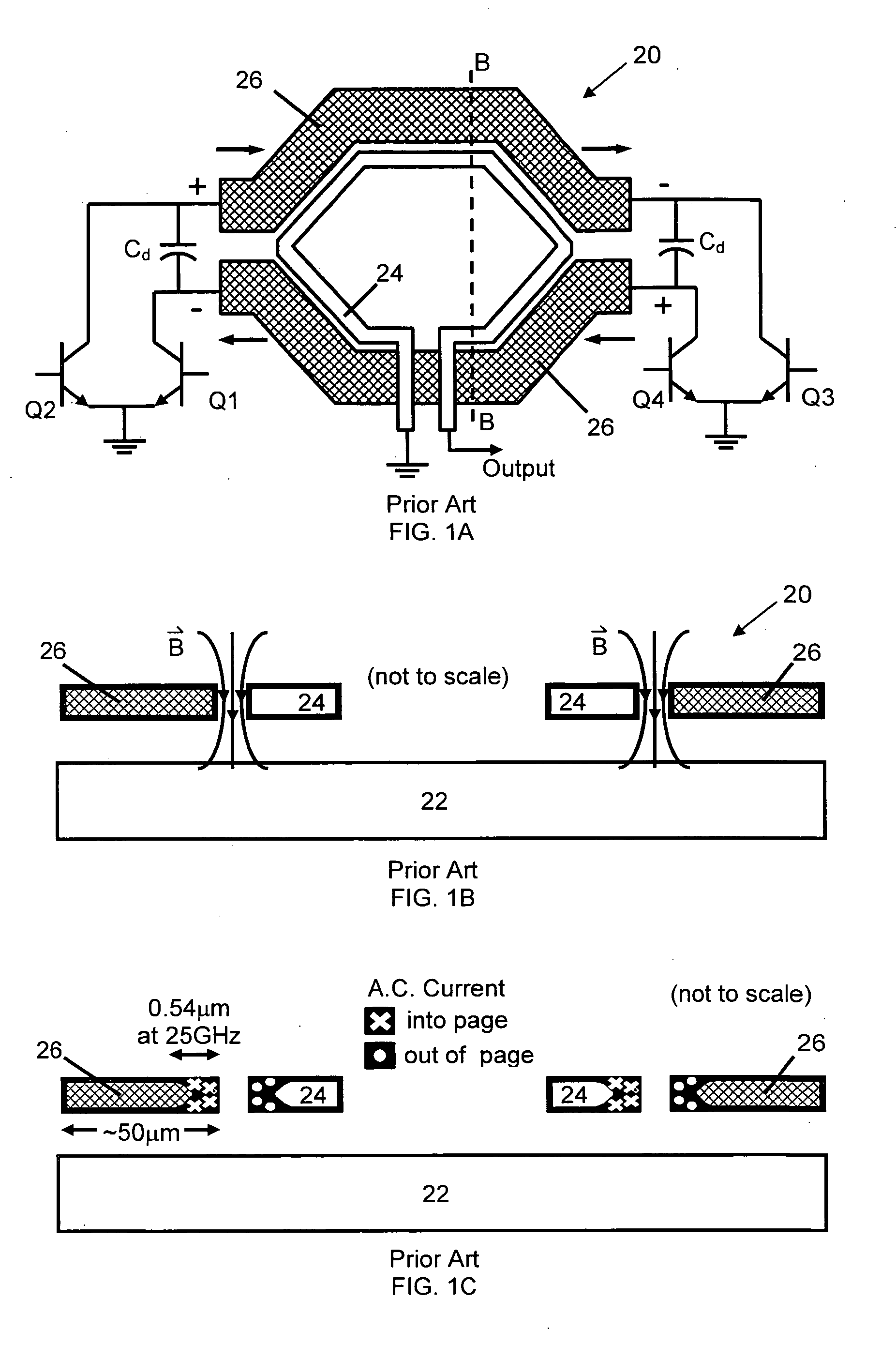
[0033]FIG. 5 is a simplified schematic diagram of a power amplifier incorporating embodiments of th...


PUM


Abstract

An electronic component including at least one first conductor for operating at a first voltage applied thereto and at least one second conductor for operating at a second voltage applied thereto. The second voltage is smaller than the first voltage and at least a portion of the second conductor is located on at least one side of the first conductor whereby the second conductor acts as a shield to substantially inhibit at least one of magnetic and electric field from passing from the first conductor to a surrounding medium.

Description

FIELD OF THE INVENTION [0001] The present invention relates generally to electronic components. More particularly, the present invention relates to shielding of passive electronic components such as inductors, transformers and balun power combiners or balun power splitters. BACKGROUND OF THE INVENTION [0002] Future broadband wireless networks will utilize integrated circuits that process radio frequency (RF) signals in bands where wavelengths may be just a few millimeters. For example, operation in the 24 GHz ISM band reduces congestion in lower frequency bands and supports data services up to hundreds of megabytes per second (Mb / s), enabling the next generation of wireless access and connectivity. Efficiency of passive electronic components is paramount when operating at radio frequencies. This is also true at millimeter wavelengths, because the quality of electronic circuit realizations depends more upon low-loss passive components as the wavelength shrinks. [0003] Implementation ...

Claims


Application Information

Patent Timeline
Patent Type & Authority Applications(United States)
IPC IPC(8): G01R31/28
CPCH03F3/211H03F3/45085H03F3/45475H05K9/0064H03F2200/06H03F2200/09H03F2203/45638H03F3/602
Inventor CHEUNG, TAK SHUNLONG, JOHN ROBERT
Owner CHEUNG TAK SHUN
Why Eureka
Try Eureka