Fabrication Method of Semiconductor Integrated Circuit Device

Inactive Publication Date: 2007-03-29
ENOMOTO HIROYUKI +2
View PDF12 Cites 223 Cited by
  • Summary
  • Abstract
  • Description
  • Claims
  • Application Information

AI Technical Summary

Benefits of technology

[0015] An object of the present invention is to provide a technique making it possible to suppress the following defects: when an interlayer insulating film including a silicon carbide film and an organic insulating film is dry-etched to form interconnection grooves over underlying Cu in

Problems solved by technology

However, the following defects were generated: an insulating reactant adhered to the surface of the underlying Cu interconnections exposed to the bottom of the

Method used


Image

  • Fabrication Method of Semiconductor Integrated Circuit Device
  • Fabrication Method of Semiconductor Integrated Circuit Device
  • Fabrication Method of Semiconductor Integrated Circuit Device

Examples


embodiment 1

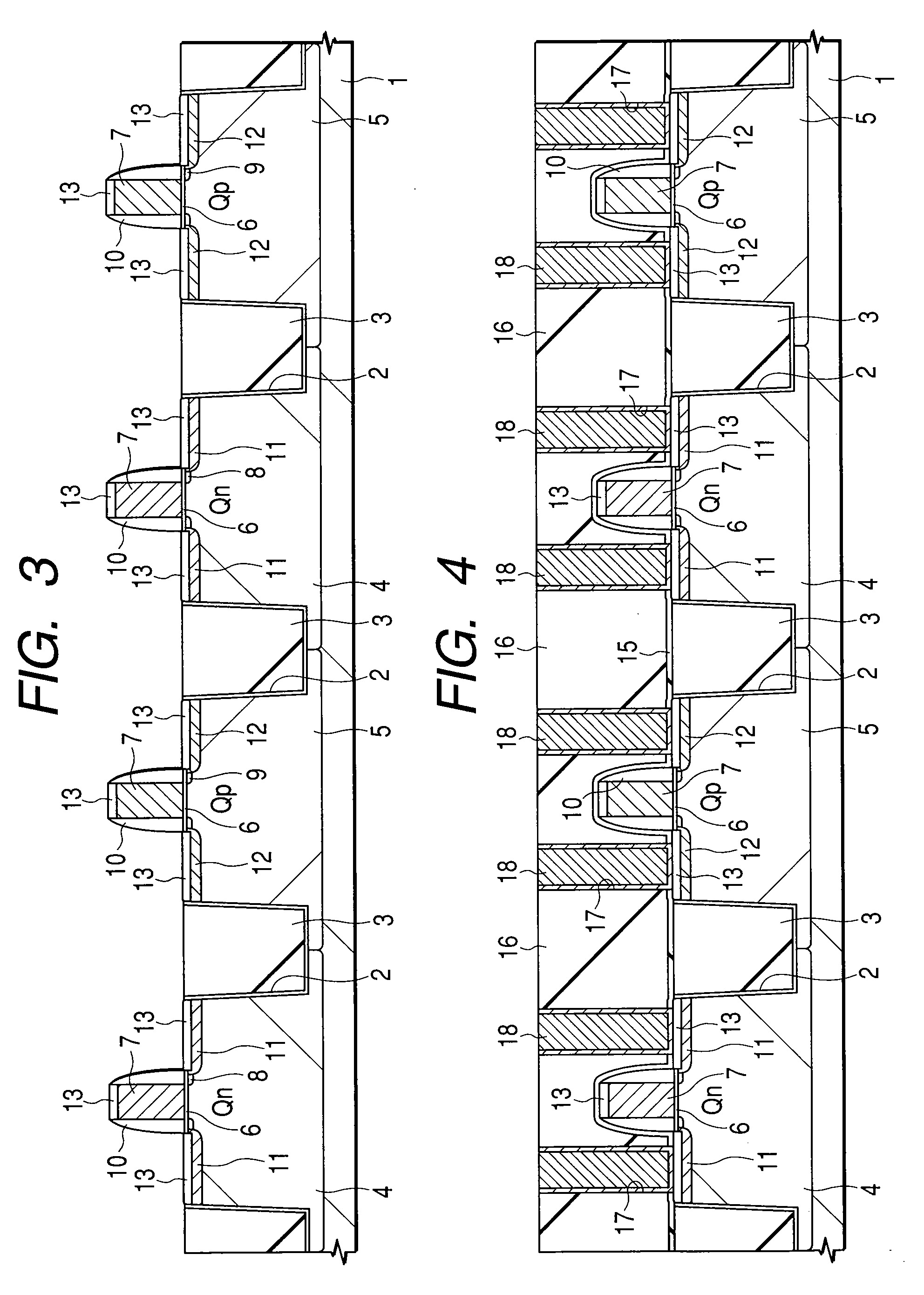
[0065] A process of fabricating a CMOS-LSI, which is an embodiment of the present invention, will be described in order of steps thereof, referring to FIGS. 1 to 15.

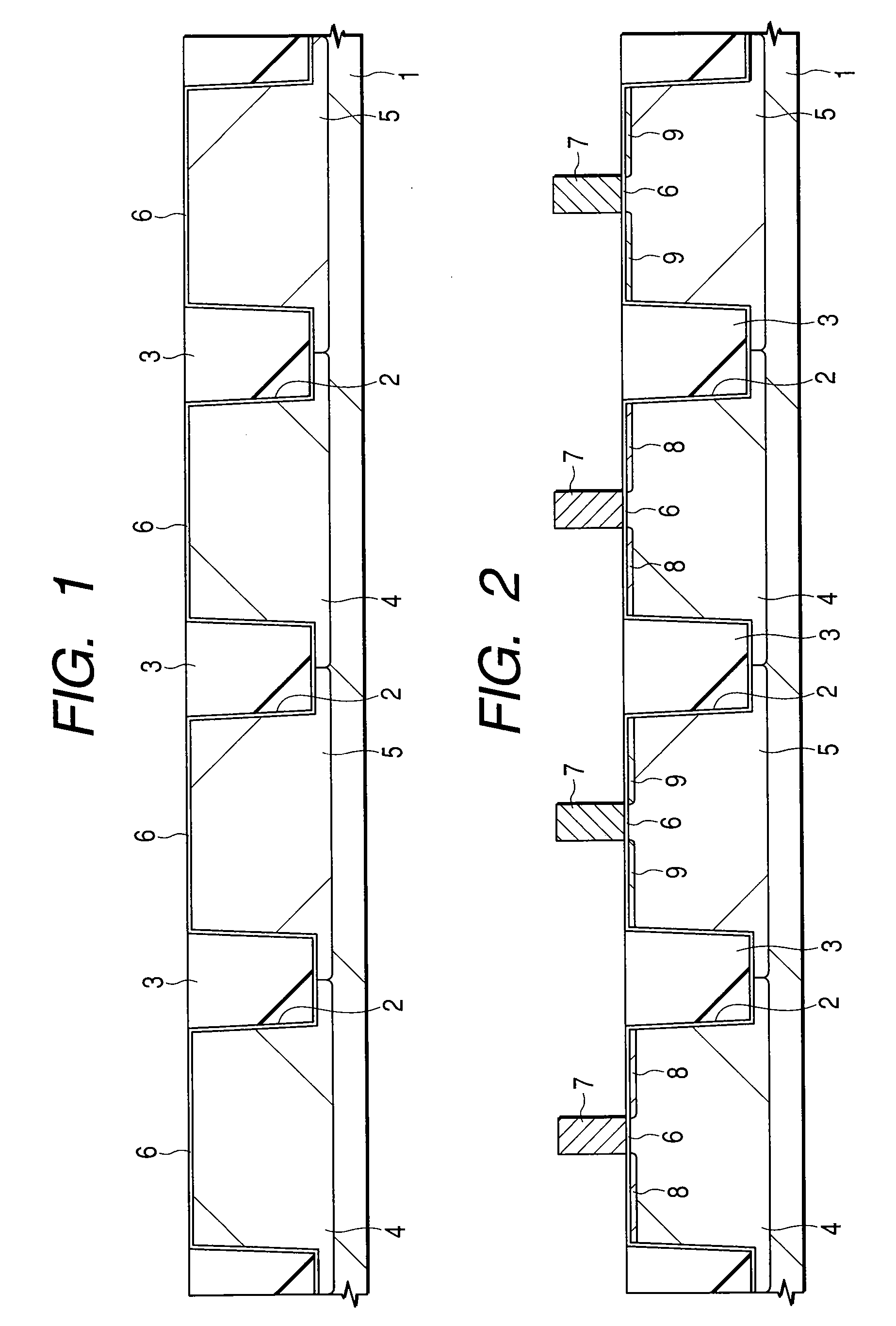
[0066] As illustrated in FIG. 1, first, element-isolating grooves 2 are made in a semiconductor substrate (hereinafter referred to as a substrate or a wafer) made of p-type monocrystal silicon having a resistivity of, for example, about 1 to 10 Ωcm. The element-isolating grooves 2 are made by etching element-isolating regions in the substrate 1 to make grooves, depositing a silicon oxide film 3 on the substrate 1 including the inside space of the grooves by CVD and subsequently polishing the silicon oxide film 3 outside of the grooves chemically and mechanically.

[0067] Next, boron is ion-implanted into some parts of the substrate 1, and phosphorous is ion-implanted into some other parts thereof to form p-type wells 4 and n-type wells 5. Thereafter, the substrate 1 is subjected to steam-oxidization to form a gate oxidiz...

embodiment 2

[0111] The following will describe, as the present embodiment, a case in which a siloxane (SiO)-based, low dielectric constant (Low-k) insulating film is used as an interlayer insulating film material and silicon nitride films are used as a diffusion barrier layer and an etching stopper layer. In the present embodiment, a SiOF film having a dielectric constant of 3.5 is used as the interlayer insulating film material. However, it is allowable to use some other inorganic or organic siloxane-based material (organic glass type insulating film), for example, HSQ (hydrogen silsesquioxane), MSQ (methyl silsesquioxane), porous HSQ, or porous MSQ.

[0112] Examples of the HSQ-based material include “OCD T-12” (made by Tokyo Ohka Kogyo Co., Ltd., dielectric constant=3.4-2.9), “FOx” (made by Dow Corning Co. in USA, dielectric constant=2.9), and “OCL T-32” (made by Tokyo Ohka Kogyo Co., Ltd., dielectric constant=2.5). Examples of the MSQ-based material include “OCD T-9” (made by Tokyo Ohka Kogyo...

embodiment 3

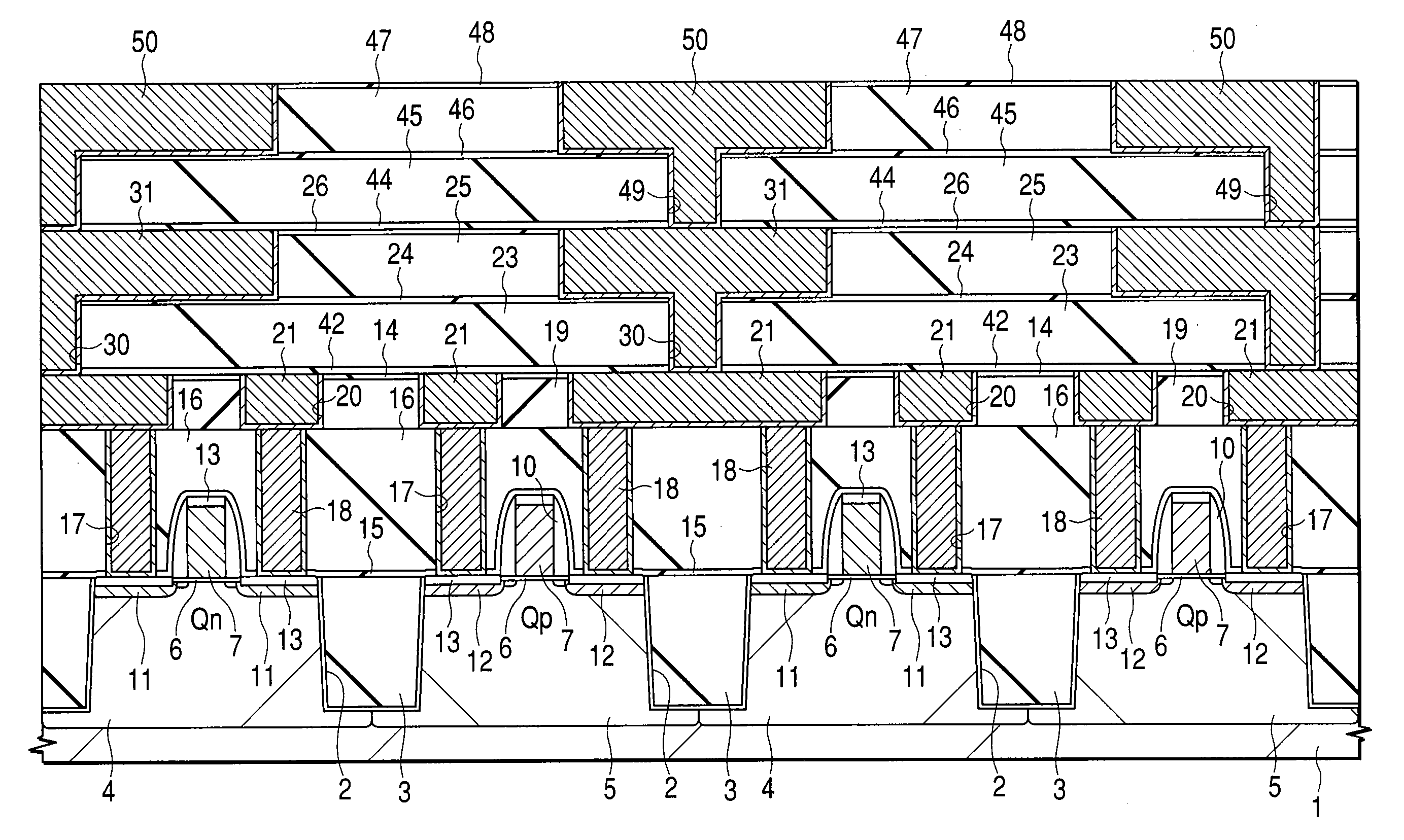
[0129] A process of fabricating a CMOS-LSI according to the present embodiment will be described in order of the steps thereof, referring to FIGS. 23 to 33.

[0130] As illustrated in FIG. 23, n-channel type MISFETs Qn and p-channel type MISFETs Qp are formed over a substrate 1. Thereafter, Cu interconnections 21 as a first layer are formed thereon. A process up to this step is the same as illustrated in FIGS. 1 to 6 about Embodiment 1.

[0131] Next, as illustrated in FIG. 24, a silicon carbonitride (SiCN) film 42, an organic insulating film 23, a silicon oxide film 24, an organic insulating film 25, a silicon oxide film 26 and a silicon carbonitride film 43 are successively deposited over the Cu interconnections 21. The silicon oxide films 24 and 26 are deposited by CVD. The organic insulating films 23 and 25 are formed by depositing an insulating material having a smaller dielectric constant than silicon oxide, for example, the above-mentioned “SiLK” or “FLARE”, by spin coating. The ...


PUM


Abstract

The following defects are suppressed: when an interlayer insulating film including a silicon carbide film and an organic insulating film is dry-etched to form interconnection grooves over underlying Cu interconnections, an insulating reactant adheres to the surface of the underlying Cu interconnections exposed to the bottom of the interconnection grooves, or the silicon carbide film or the organic insulating film exposed to the side walls of the interconnection grooves are side-etched. When a lamination film made of a silicon oxide film, an organic insulating film, a silicon oxide film, an organic insulating film and a silicon carbide film is dry-etched to form interconnection grooves over Cu interconnections, a mixed gas of SF6 and NH3 is used as an etching gas for the silicon carbide film to work side walls of the interconnection grooves perpendicularly and further suppress defects that a deposit or a reactant adheres to the surface of the Cu interconnections exposed to the bottom of the interconnection grooves.

Description

BACKGROUND OF THE INVENTION [0001] The present invention relates to a technique on fabrication of a semiconductor integrated circuit device, particularly a technique effective for the formation of a copper interconnection, using Damascene process. [0002] In recent processes of fabricating a semiconductor integrated circuit device wherein circuits are made highly fine and integrated to a very high degree, element-isolating trenches are made in a silicon substrate or contact holes are made in self-alignment to gate elements of metal insulator semiconductor field effect transistors (MISFETs), for example, by using a difference in etching speed between different kinds of insulating films, such as a silicon oxide film and a silicon nitride film. [0003] Japanese Patent Unexamined Publication No. Hei 10(1998)-321838 discloses a technique of depositing a silicon oxide film across a silicon carbide (SiC) film over a gate electrode to which a side wall spacer made of a silicon oxide film or a...

Claims


Application Information

Patent Timeline
IPC IPC(8): H01L21/4763H01L21/3065H01L21/311H01L21/768
CPCH01L21/31116H01L21/31138H01L21/76832H01L21/76813H01L21/76811
Inventor ENOMOTO, HIROYUKITAGO, KAZUTAMIMAEKAWA, ATSUSHI
Owner ENOMOTO HIROYUKI
Why Eureka
Try Eureka