

Plasma CVD apparatus and plasma surface treatment method
a plasma surface treatment and plasma technology, applied in the direction of coatings, electric discharge tubes, metal material coating processes, etc., can solve the problems of easy drastic change of temperature of the substrate surface, only moderate change of film quality, etc., and achieve the effect of lowering the temperature of the process targ
- Summary
- Abstract
- Description
- Claims
- Application Information
AI Technical Summary
Benefits of technology
Problems solved by technology
Method used
Image

Examples
Embodiment Construction
[0056] An embodiment of the present invention will be specifically explained below with reference to the drawings.
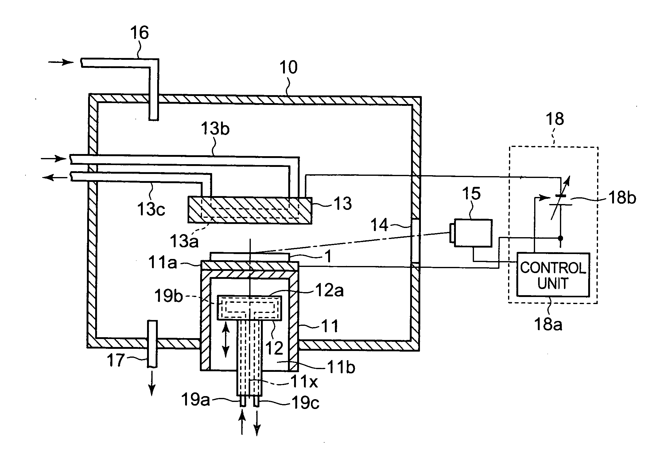
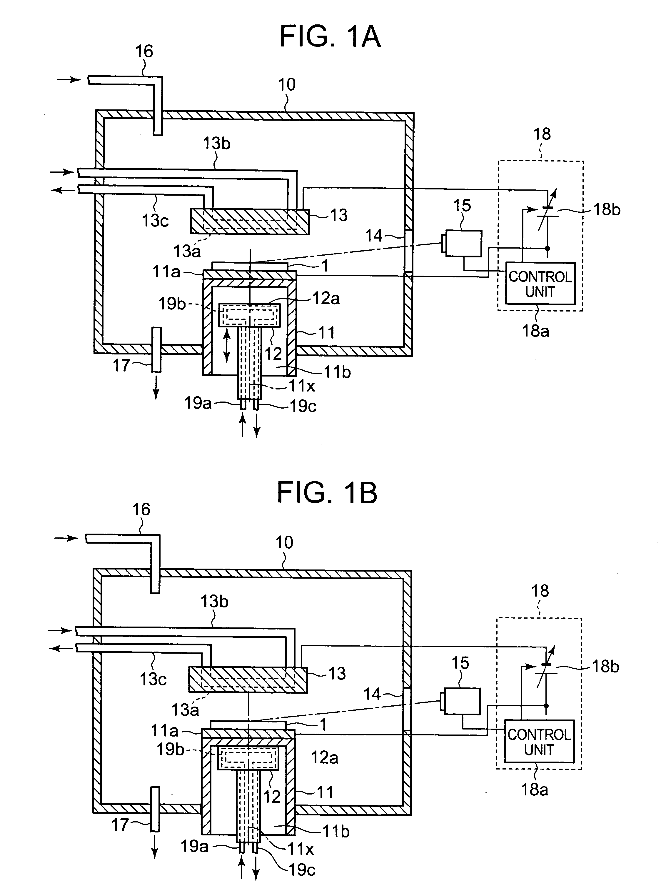
[0057]FIG. 1A and FIG. 1B are structure diagrams showing the overview of a direct-current (DC) plasma CVD apparatus according to an embodiment of the plasma CVD apparatus according to the present invention.
[0058] The DC plasma CVD apparatus is for forming a film on the surface of a substrate 1 as a process target, and comprises a chamber 10 for shielding the substrate 1 from the external atmosphere.
[0059] A stage 11 made of steel is arranged inside the chamber 10. An anode 11 a made of a high melting point metal having a disk shape and a fine thermal conductivity is mounted on the stage 11. The substrate 1 is fixed on the upper mount surface of the anode 11a. The stage 11 is set to rotate together with the anode 11a about an axis 11x. Molybdenum (thermal conductivity: 138 W / m·K, melting point: 2620° C.) is preferred as the metal of the anode 11a.
[0060] A closed space...
PUM
| Property | Measurement | Unit |
|---|---|---|
| Temperature | aaaaa | aaaaa |
| Temperature | aaaaa | aaaaa |
| Flow rate | aaaaa | aaaaa |
Abstract
Description
Claims
Application Information