
Display device

a display device and display circuit technology, applied in the field of display devices, can solve the problems of increasing the manufacturing cost of the drive control circuit, increasing the manufacturing cost of the display device, and similar problems in the a-si tft but also in the organic tft, so as to prevent the variation of the threshold voltage of the tft

Inactive Publication Date: 2007-04-05
MITSUBISHI ELECTRIC CORP
View PDF0 Cites 10 Cited by
  • Summary
  • Abstract
  • Description
  • Claims
  • Application Information

AI Technical Summary

Benefits of technology

[0009] It is an object of the present invention to provide a display device which is able to prevent variation in a threshold voltage of a TFT of a gate driver with the use of a general-purpose drive control circuit.
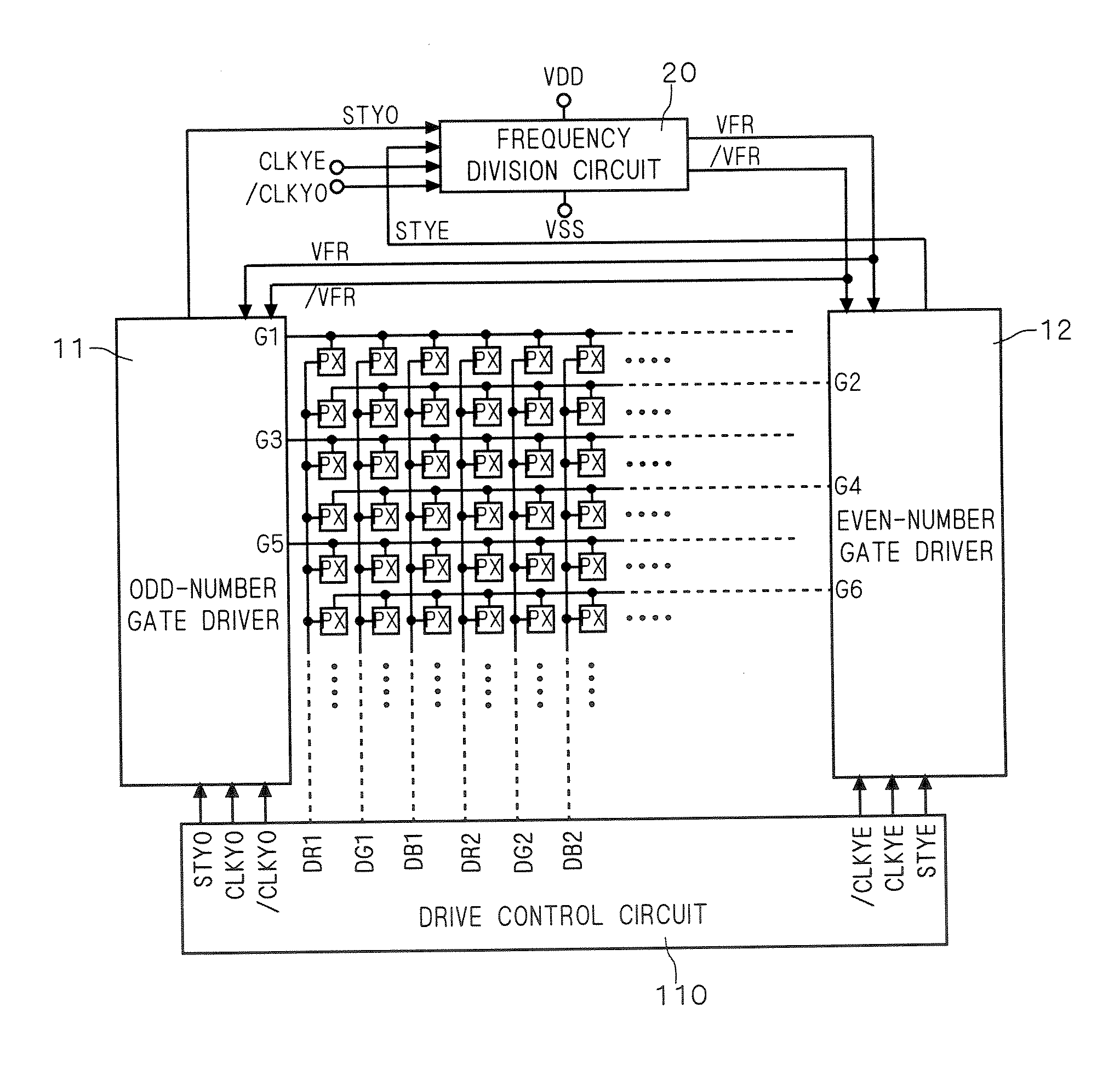
[0011] It is possible to switch between two output pull-down TFTs included in the gate driver from frame to frame based on the frequency division circuit. The frequency division signal is obtained by dividing a frequency of each of two start signals output from a general-purpose drive control circuit. Thus, a gate driver of a type in which two output pull-down TFTs are switched from frame to frame can be actuated by using a general-purpose drive control circuit. Accordingly, it is possible to prevent malfunction which is likely to occur due to variation in a threshold voltage of a TFT of the gate driver while suppressing an increase in costs associated with the display device. Also, the frequency division circuit is formed using the TFTs formed on the same substrate in which the TFTs used for forming the pixels and the gate driver are formed. Hence, complication of manufacturing processes which may be caused due to inclusion of the frequency division circuit in the display device can be avoided.

Problems solved by technology

That phenomenon probably causes malfunction of a gate driver formed using an a-Si TFT, to present a problem.
Also, it has been found that a similar problem arises in not only an a-Si TFT but also an organic TFT.
However, an LSI of a general-purpose drive control circuit which has conventionally been used does not output a control signal (switching signal) for switching a state of each of the foregoing two a-Si TFTs for pulling down an output, between an operative state and an inoperative state from frame to frame.
This increases manufacturing costs associated with the drive control circuit, and thus increases manufacturing costs associated with a display device.

Method used


Image

  • Display device
  • Display device
  • Display device

Examples


first preferred embodiment

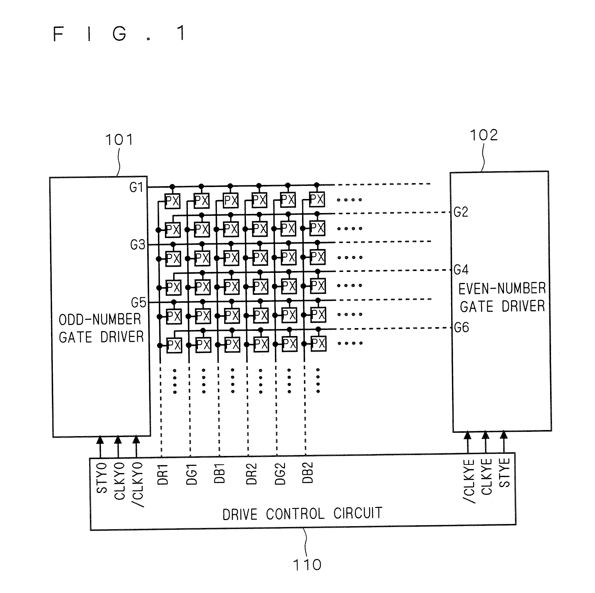
[0038] Specific preferred embodiments of the present invention will be described as follows. However, as a preliminary, a conventional general-purpose drive control circuit and a conventional general-purpose gate driver will be described for the sake of easier understanding of the present invention. FIG. 1 is a block diagram illustrating an example of a structure of a conventional display device.

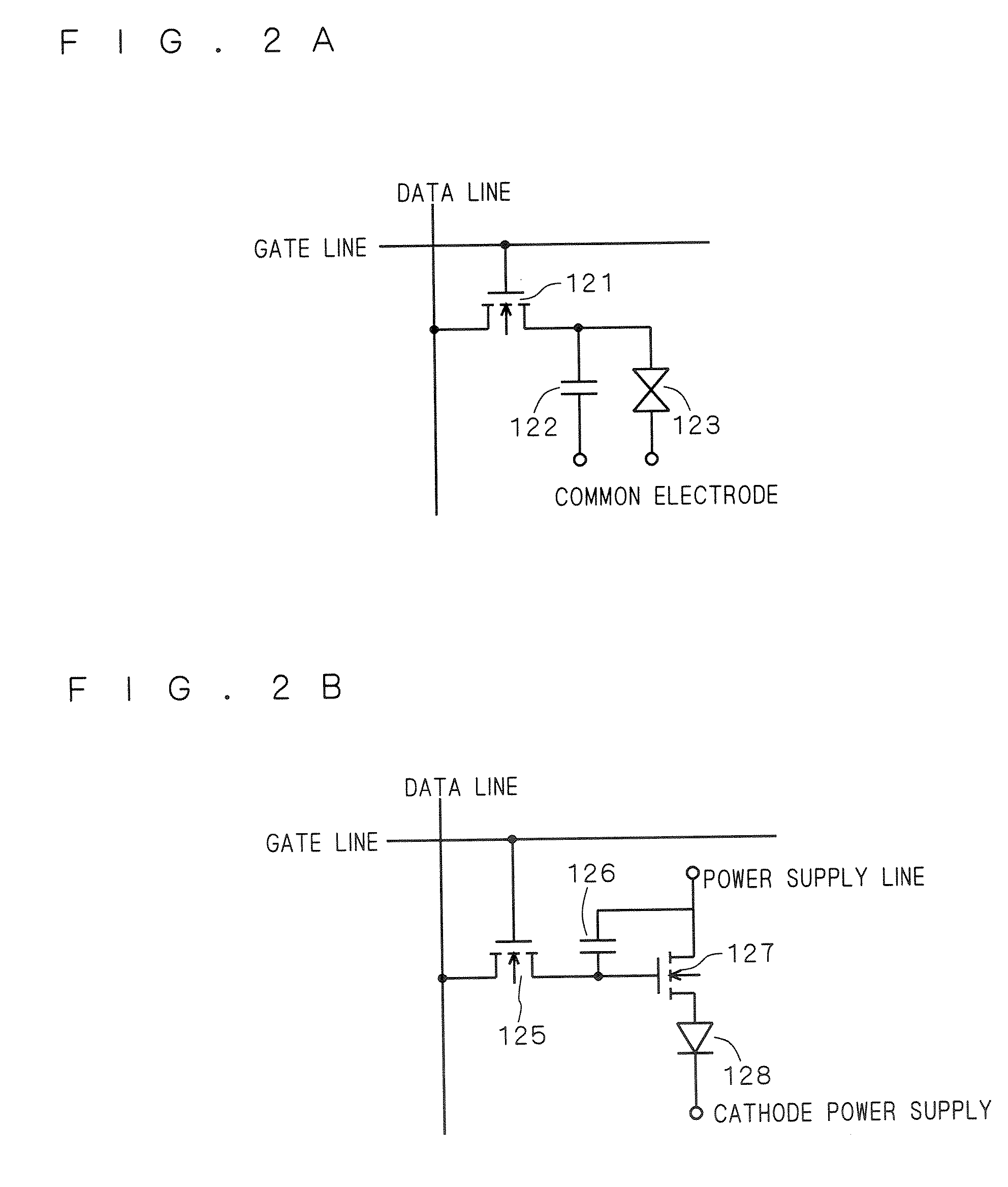
[0039] In the display device illustrated in FIG. 1, pixels PX formed using a-Si TFTs which are formed on an insulating substrate such as a glass substrate are arranged in a matrix. As an example of the pixels PX, a pixel formed using a liquid crystal element and a pixel formed using an electroluminescent element such as an organic electroluminescent (EL) element are cited, for example.

[0040]FIG. 2A illustrates an example of a structure of a liquid crystal pixel formed using a-Si TFTs. A gate line is connected with a gate of an active element 121 (a-Si TFT) and a data line is connected with...

second preferred embodiment

[0125] In a second preferred embodiment, an example of a circuit configuration for the frequency division circuit 20, which is different from the circuit configuration illustrated in FIG. 7, will be described. FIG. 12 illustrates a circuit configuration of a frequency division circuit 20a according to the second preferred embodiment.

[0126] The frequency division circuit 20a is different from the frequency division circuit 20 in FIG. 7 in that a transistor Q26 is provided between the input terminal for the start signal STYE and the node N5. More specifically, the frequency division circuit 20a includes a latch / inverter 23a including the transistors Q10, Q11, Q12, Q13, and Q26, in place of the latch / inverter 23 in FIG. 7, between the node N1 and the node N5.

[0127]FIG. 13 is a timing chart showing operations of the frequency division circuit 20a. More specifically, operations performed while the frequency division signals VFR and / VFR are transitioning from H level and L level to L l...

third preferred embodiment

[0129] Also in a third preferred embodiment, an example of a circuit configuration for the frequency division circuit 20, which is different from the circuit configuration illustrated in FIG. 7, will be described. FIG. 14 illustrates a circuit configuration of a frequency division circuit 20b according to the third preferred embodiment. The frequency division circuit 20b in FIG. 14 includes a buffer 29 in place of the transistor Q1 in FIG. 7, and further includes a buffer 22a in place of the buffer 22 and the transistor Q9 in FIG. 7. The circuit configuration of the frequency division circuit 20b is identical to that in FIG. 7 in all the other respects.

[0130] The buffer 29 includes a buffer circuit including transistors Q18a and Q19a, a transistor Q1a connected between the buffer circuit and the input terminal for the start signal STYO, and a transistor Q1b connected between the buffer circuit and the low level power supply. A gate of the transistor Q18a is connected with the gate ...


PUM


Abstract

A display device includes a gate driver for driving pixels (PX), a drive control circuit for outputting a predetermined control signal to the gate driver, and a frequency division circuit. The pixels, the gate driver, and the frequency division circuit are formed using amorphous silicon thin film transistors (a-Si TFTs) formed on an insulating substrate. The control signal output from the drive control circuit includes a start signal for a start of a frame period of an image signal, and the frequency division circuit generates a frequency division signal whose period corresponds to a frequency which is obtained by dividing a frequency of the start signal.

Description

BACKGROUND OF THE INVENTION [0001] 1. Field of the Invention [0002] The present invention relates to a display device including a gate driver which includes a thin film transistor (TFT). [0003] 2. Description of the Background Art [0004] A display device such as a liquid crystal display or an organic electroluminescent (EL) display includes pixels arranged in a matrix on an insulating substrate such as a glass substrate, gate lines (scanning lines) respectively provided for rows of the pixels (pixel lines), and a gate driver for selecting and driving the gate lines one by one. A gate driver can be formed using a shift register. In this regard, it is desirable that a shift register used for forming a gate driver includes only field effect transistors of the same conductivity type, for purposes of simplifying manufacturing processes. Hence, various types of shift registers each of which includes only n-channel or p-channel field effect transistors have been suggested, along with vario...

Claims


Application Information

Patent Timeline
IPC IPC(8): G09G3/36
CPCG09G3/20G09G2300/0408G09G2300/08G09G2310/0267G11C19/28H03K5/15093G02F1/136G09G3/30G09G3/36
Inventor TOBITA, YOUICHI
Owner MITSUBISHI ELECTRIC CORP
Learn More