Semiconductor memory device

a memory device and semiconductor technology, applied in the field of semiconductor integrated circuits, can solve the problems of increased power consumption, operational failure, and degraded operating stability of power supply voltage, and achieve the effects of improving operating speed, reducing leakage current, and improving performance characteristics

Active Publication Date: 2007-04-05
RENESAS ELECTRONICS CORP
View PDF10 Cites 66 Cited by
  • Summary
  • Abstract
  • Description
  • Claims
  • Application Information

AI Technical Summary

Benefits of technology

[0009] The power supply voltage of LSIs (Large Scale Integrated Circuits) has been reduced to reduce the power consumption and the size of their transistors. For example, the 90 nm process produces LSIs operating at a power supply voltage of 1.2 V. In the case of an SRAM circuit, a reduction in the power supply voltage degrades the operating stability during read and write operations, which may result in operational failure. If the driving power (or current) of each transistor making up a memory cell changes, so does the performance of the cell in terms of stability of read and write operations and operating speed.
[0010] Therefore, the performance characteristics of each transistor in a memory cell may be appropriately controlled to maximize the performance of the cell. Reducing the power supply voltage of the cell results in a reduction in the drive current of the transistors and in the operating speed of the circuit. To prevent such a reduction in the operating speed when the power supply voltage is lowered, the threshold voltage (Vth) of the transistors may be reduced to maintain their operating current level.
[0011] However, reducing the threshold voltage (Vth) of a transistor increases the leakage current flowing between the source and drain of the transistor in the off state (or when it is turned off), resulting in increased power consumption. (This leakage current is referred to as a “subthreshold leakage current”.) The technique disclosed in the above patent document 1 controls the substrate potential of appropriate transistors in an SRAM memory cell and thereby controls the performance of these transistors in order to reduce their power consumption in the off state. More specifically, in the case of an n-channel bulk CMOS transistor, a voltage lower than the source electrode voltage may be applied to the back gate to increase the threshold voltage Vth of the transistor and thereby reduce the subthreshold leakage current.

Problems solved by technology

For example, the 90 nm process produces LSIs operating at a power supply voltage of 1.2 V. In the case of an SRAM circuit, a reduction in the power supply voltage degrades the operating stability during read and write operations, which may result in operational failure.
However, reducing the threshold voltage (Vth) of a transistor increases the leakage current flowing between the source and drain of the transistor in the off state (or when it is turned off), resulting in increased power consumption.
However, if the back gate of a scaled-down bulk CMOS transistor manufactured by a 90 nm or less process is controlled in such a manner, the leakage current flowing from the drain electrode to the substrate electrode (called the junction leakage current) increases.

Method used


Image

  • Semiconductor memory device
  • Semiconductor memory device
  • Semiconductor memory device

Examples


first embodiment

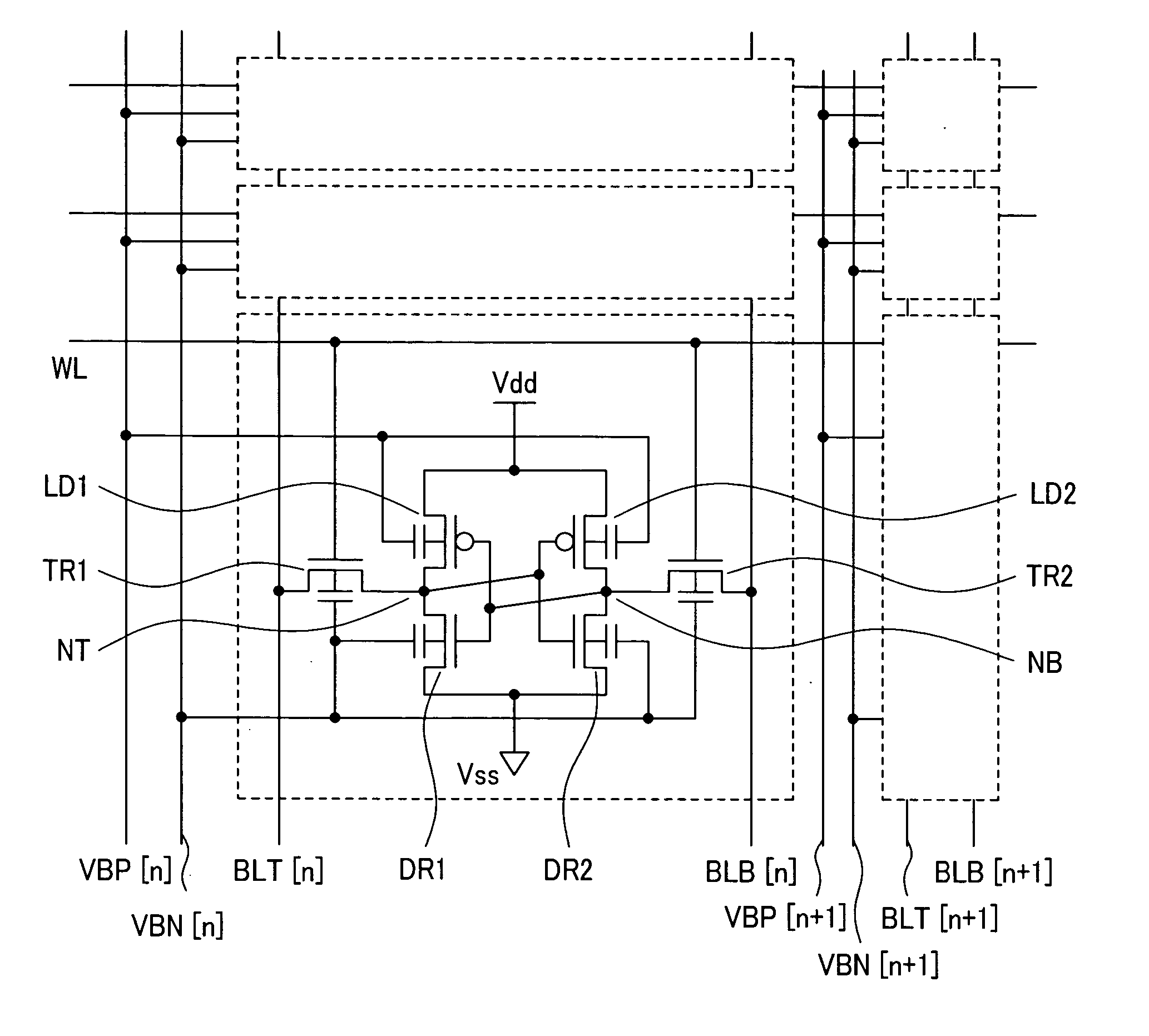
[0061]FIG. 1 shows a circuit diagram of an SRAM circuit according to a first embodiment of the present invention. In the figure, [n] indicates the nth column and [n+1] indicates the (n+1)th column. For example, VBN[n] denotes an n-well node to which are connected the wells of the nMOS transistors in all nth-column memory cells (as described below). Such a notation will be used as necessary throughout this specification. Referring to FIG. 1, symbols BLT and BLB denote bit lines; WL, a word line; Vdd, a high level power supply line; Vss, a ground line; NT and NB, data storage nodes for storing data; TR1 and TR2, transfer transistors connected between the bit lines and the data storage nodes; DR1 and DR2, drive transistors for driving the data storage nodes to a low level; LD1 and LD2, load transistors for supplying charge to the data storage nodes; VBN[n], a node to which are connected the well nodes of the nMOS transistors in all nth-column memory cells; and VBP[n], a node to which a...

second embodiment

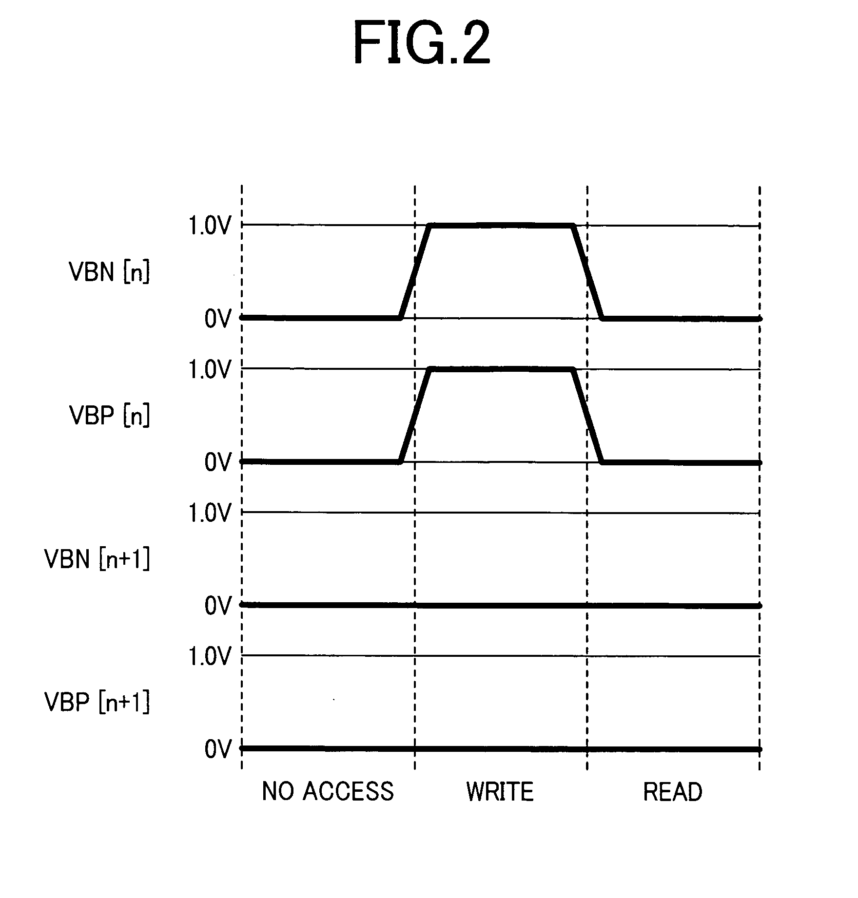
[0083]FIG. 13 shows an example of how to control well potentials of an SRAM memory cell according to a second embodiment of the present invention. It should be noted that in the following description of preferred embodiments, components identical to those of the first embodiment will be denoted by like numerals and only other components will be described. The circuit configuration of this memory cell is the same as that shown in FIG. 1 in terms of transistor arrangement. FIG. 13 is different from FIG. 2 in that in the “No access” state (in which the memory cell is not accessed), the well potential of the pMOS transistors is set to a high level. In the “No access” state, especially in the stand-by state in which the memory cell stores data but is not accessed, the leakage current of the memory cell may cause a problem. In this state, if the well potential of the pMOS transistors is set to a low level, a large leakage current flows since the threshold voltages Vth of the pMOS transist...

third embodiment

[0084]FIG. 14 shows a circuit diagram of an SRAM circuit according to a third embodiment of the present invention. The memory cell of the present embodiment is different from that of the first embodiment in that it includes two n-well nodes VBN1 and VBN2, instead of only one n-well node (i.e., the node VBN). The node VBN1 is connected to the wells of the nMOS transistors (on the left side) that are connected in series between the bit line BLT and the node Vss; and the node VBN2 is connected to the wells the nMOS transistors (on the right side) that are connected in series between the bit line BLB and the node Vss. The layout of the memory cell is the same as that shown in FIG. 5. (The layout of the memory cell need not be changed, since in the arrangement shown in FIG. 5, the well nodes of the nMOS transistors on the right and left sides are already connected separately.)

[0085]FIG. 15 shows the (voltage) waveform of each portion (or node) of the circuit of the present embodiment. T...


PUM


Abstract

An object of the present invention is to provide a technique of reducing the power consumption of an entire low power consumption SRAM LSI circuit employing scaled-down transistors and of increasing the stability of read and write operations on the memory cells by reducing the subthreshold leakage current and the leakage current flowing from the drain electrode to the substrate electrode. Another object of the present invention is to provide a technique of preventing an increase in the number of transistors in a memory cell and thereby preventing an increase in the cell area. Still another object of the present invention is to provide a technique of ensuring stable operation of an SRAM memory cell made up of SOI or FD-SOI transistors having a BOX layer by controlling the potentials of the wells under the BOX layers of the drive transistors.

Description

CLAIM OF PRIORITY [0001] The present application claims priority from JP2005-290889, filed on Oct. 4, 2005, the content of which is hereby incorporated by reference into this application. BACKGROUND OF THE INVENTION [0002] 1. Field of the Invention [0003] The present invention relates to a semiconductor integrated circuit in which a static memory (SRAM) circuit is integrated on a semiconductor chip, and more particularly to a configuration of an SRAM integrated circuit device that allows operating margins to be increased. [0004] 2. Description of the Related Arts [0005] In recent years, there has been a strong need to increase the speed of semiconductor devices such as SRAM circuits, as well as reducing their power consumption. [0006]FIG. 32 shows a conventional SRAM memory cell circuit. Referring to the figure, symbols BLT and BLB denote bit lines; WL, a word line; Vdd, a high level power supply line; and Vss, a ground line. Further, reference numerals 201 and 202 denote transfer t...

Claims


Application Information

Patent Timeline
Patent Type & Authority Applications(United States)
IPC IPC(8): G11C11/00
CPCG11C11/412G11C5/025G11C5/063G11C11/419
Inventor YAMAOKA, MASANAOKAWAHARA, TAKAYUKI
Owner RENESAS ELECTRONICS CORP
Why Eureka
Try Eureka