

Surface mounting semiconductor device
a semiconductor and surface mounting technology, applied in semiconductor devices, solid-state devices, electrical apparatus construction details, etc., can solve the problems of poor reliability of solder joints, large influence on the efficiency reduction of light emission, poor state, etc., and achieve reliable mounting on circuit boards, good mounting properties, and stable state
- Summary
- Abstract
- Description
- Claims
- Application Information
AI Technical Summary
Benefits of technology
Problems solved by technology
Method used
Image

Examples
Embodiment Construction
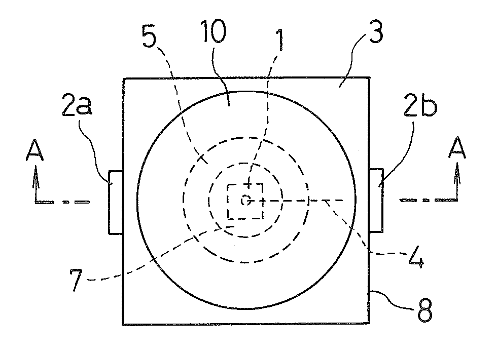
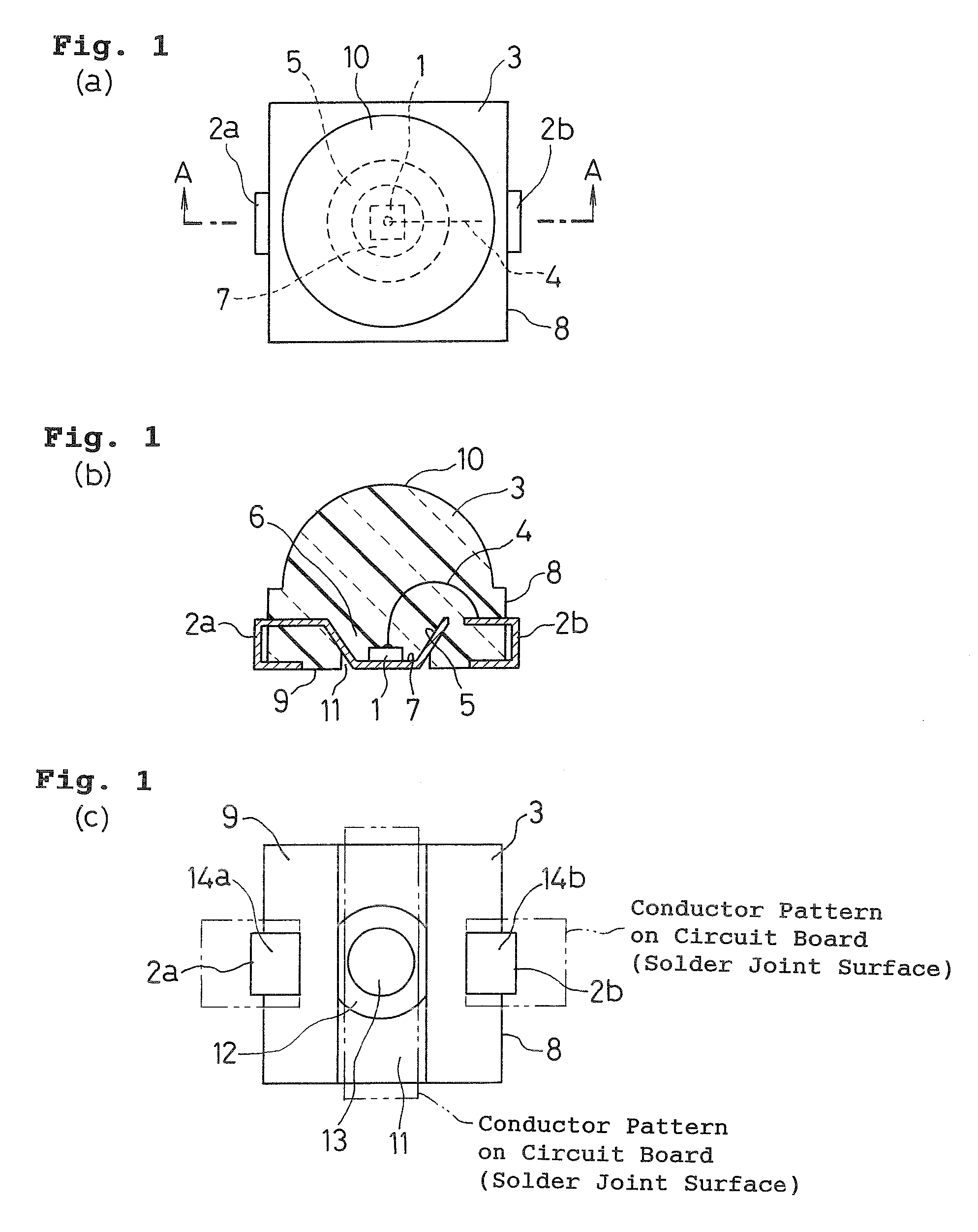
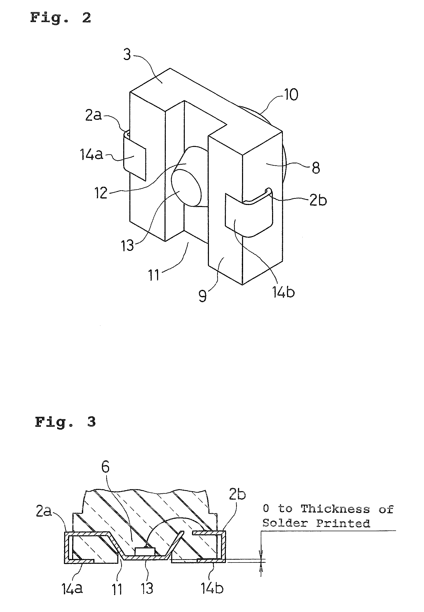
[0041] A surface mounting semiconductor device having nice mounting properties with good mounting reproducibility, excellent resistance to different environments, good thermal radiation properties, optical properties and electrical properties, high reliability, and / or other advantageous features is possible according to the disclosed subject matter herein. A semiconductor element can be mounted on an inner bottom surface of a recess formed in a lead frame and sealed in a resin. An outer bottom surface and an outer circumferential surface of the recess can be at least partly externally exposed from the sealing resin. The exposed portion(s) of the recess can be bonded to conductor patterns on a circuit board via a bonding agent having electrical conduction and / or thermal conduction. Such mounting can be adopted to achieve the above-noted features of the disclosed subject matter.
[0042] Exemplary embodiments of the disclosed subject matter will now be described in detail with reference...
PUM
 Abstract
Description
Claims
Application Information