Switch block for FPGA architectures

a technology of fpga architecture and switch block, which is applied in the direction of logic circuits using elementary logic circuit components, electrical apparatus, solid-state devices, etc., can solve the problems of static power being the dominant factor in energy consumption, the architecture is affected more heavily, and the integrated circuit leakage current is exposed, so as to reduce the static consumption of the architecture

Active Publication Date: 2007-04-19
STMICROELECTRONICS SRL
View PDF7 Cites 13 Cited by
  • Summary
  • Abstract
  • Description
  • Claims
  • Application Information

AI Technical Summary

Benefits of technology

[0051] The disclosed embodiments of the present invention are directed to a switch block for FPGA architectures having structural and functional characteristics, which provide reduced static consumption of the architecture as a whole without affecting the operational speed thereof, and in this way overcoming the limits that still affect the devices realized according to the known designs.

Problems solved by technology

As it is well known, technology scaling is leading to an exponential increase in integrated circuit leakage current, such that below 90 nm static power could be the dominant factor in energy consumption.
In particular, configurable structures such as FPGA (Field-Programmable Gate Arrays) architectures are affected more heavily than other devices such as ASICs by this problem, since they require many more transistors to support their main feature, the reconfigurability.
However, as technology scales the area constraint is becoming less restrictive, while the large number of integrated transistors in FPGA architectures is still a source of higher energy consumption of such architectures than the ASIC ones.
Since reconfigurable computing is a promising technology for wireless applications where systems need to support a variety of changing communication protocols, the power consumption constraint is becoming the main issue that could prevent FPGA architectures from being widely used in this field.
When power consumption of a FPGA architecture 1 is considered, it is immediately evident that a large part of the device area is often left completely unused when a specific circuit is mapped, and its power consumption is useless.
This is mainly due to the threshold voltage scaling which leads to an exponential increase in the subthreshold leakage.
Since leakage generates static power consumption which depends on the number of integrated transistors, FPGA architectures will be suffering from this problem even more than other devices.
These parts of the configurable device do not present dynamic power consumption but contribute to increased energy dissipation, having a static subthreshold current.
Since the percentage of total power dissipation due to leakage depends on the number of unused resources, in FPGA architectures the leakage power consumption can become relevant and energy efficiency can be deeply affected.
However this technique significantly affects delays and could be used only for non-timing critical circuits.
Though the above described dual threshold approach has been adopted, it has been verified that yet considerable power dissipation due to leakage remains, which has been measured to be more than 25 mW for a PiCoGA configurable device area occupation of 11 mm2.
This is a static consumption and scaling to technology below 100 nm will considerably increase it.
On the other hand, switch blocks and output connect blocks drive routing wires crossing over several tiles, therefore the parasitic capacitive load involved is considerable.
It is clear that this solution certainly reduces the leakage power consumption drastically, but at the cost of introducing many slow transistors on the signal path delay.

Method used


Image

  • Switch block for FPGA architectures
  • Switch block for FPGA architectures
  • Switch block for FPGA architectures

Examples


first embodiment

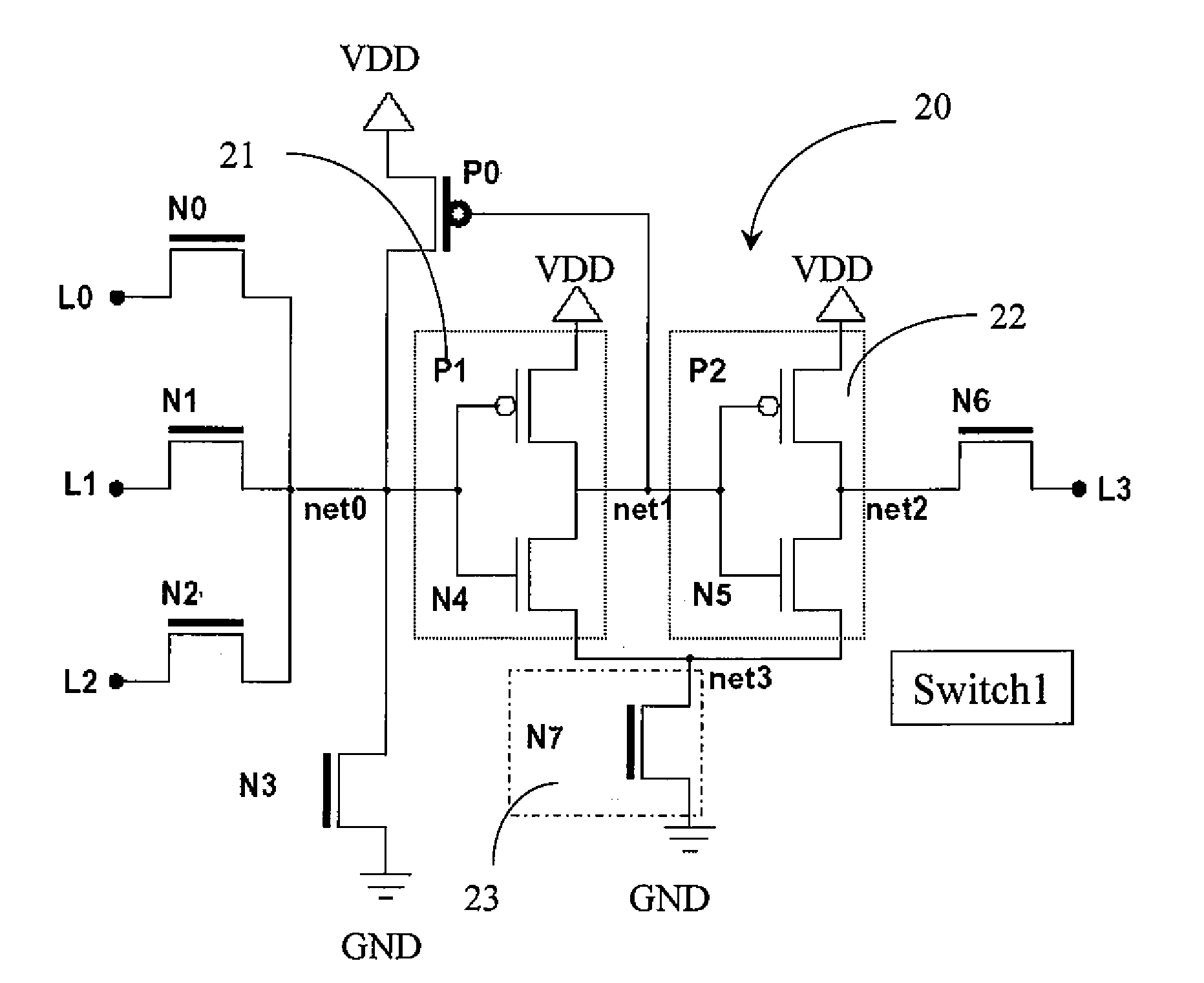
[0127] With reference to such figures, and in particular to FIG. 5, a switch block realized according to the invention is schematically shown and globally indicated as 20 or Switch1.

[0128] For structurally or functionally equal elements with respect to the switch block described in the Background section, the same reference numbers will be applied.

[0129] As already described, the switch block 20 (Switch1) realizes the connection between a first line L0, a second line L1, a third line L2 and a fourth line L3 and includes:

[0130] a first pass-transistor N0 connected between the first line L0 and a first internal node net0;

[0131] a second pass-transistor N1 connected between the second line L1 and the first internal node net0;

[0132] a third pass-transistor N2 connected between the third line L2 and the first internal node net0; and

[0133] a fourth pass-transistor N6 connected between the fourth line L3 and a second internal node net2.

[0134] In the example shown in FIG. 5, the pass-...

second embodiment

[0149] Also, advantageously according to the invention, the switch block 20 is provided, showing an enhanced driving factor with respect to the Switch1 scheme.

[0150] This second embodiment is shown in FIG. 6, globally indicated as 20 or Switch2. It will be clear from the following description that the switch block 20 (Switch2) scheme has been designed in order to reduce the propagation delay of the switch block 20 (Switch0) scheme.

[0151] The switch block 20 (Switch2) shows a similar structure with respect to the known switch block (Switch0), the detailed description thereof being so omitted for sake of simplicity, only the differences being highlighted.

[0152] In particular, the NMOS transistor N5 of the second inverter 22 is directly connected to the fourth line L3, such that the pull down path of the buffer final stage according to such Switch2 scheme comprises only the transistor N5 itself.

[0153] Moreover, the pull down transistor N3 is substituted by a further pull-up transist...

third embodiment

[0163] Advantageously with the invention, the switch block contribution to the leakage consumption of a FPGA architecture tile becomes negligible with respect to the other blocks. The same circuital scheme can also be applied for the output connect blocks, which cause most of the connect blocks dissipation.

[0164] The penalty to be paid for a low-leakage design is about 25% on the interconnect delay under same driving width conditions. Wider transistors could however be used in order to reduce this gap, all the more that the leakage advantage would remain substantially unchanged.

[0165] The switch block 20 (Switch3) also achieves the best performance, since it reduces the active leakage while keeping steep signal edges.

[0166] From an area occupation point of view, the introduction of the additional pull-down block 23, and in particular of the footer transistor N7 in the switch blocks according to the Switch1 and Switch3 schemes, increases the switch area of 37%, if considering also ...


PUM


Abstract

A switch block for FPGA architectures combining hardware and software techniques in order to reduce both active and standby leakage power.

Description

BACKGROUND OF THE INVENTION [0001] 1. Field of the Invention [0002] The present invention relates to a switch block for FPGA architectures. [0003] 2. Description of the Related Art [0004] As it is well known, technology scaling is leading to an exponential increase in integrated circuit leakage current, such that below 90 nm static power could be the dominant factor in energy consumption. [0005] In particular, configurable structures such as FPGA (Field-Programmable Gate Arrays) architectures are affected more heavily than other devices such as ASICs by this problem, since they require many more transistors to support their main feature, the reconfigurability. [0006] Indeed, configurable logic structures have become a valid alternative to ASICs because of the provided software programmability which reduces the design cycle, while density and running frequency greatly increase. It is well known that this flexibility is achieved at the cost of a larger silicon area occupation to accom...

Claims


Application Information

Patent Timeline
Patent Type & Authority Applications(United States)
IPC IPC(8): H03K19/177
CPCH03K19/177
Inventor CICCARELLI, LUCALODI, ANDREAGIANSANTE, ROBERTOMAGAGNI, LUCACANEGALLO, ROBERTOGUERRIERI, ROBERTO
Owner STMICROELECTRONICS SRL
Why Eureka
Try Eureka