Method and arrangement in inverter

Active Publication Date: 2007-05-03
ABB (SCHWEIZ) AG
View PDF4 Cites 10 Cited by
  • Summary
  • Abstract
  • Description
  • Claims
  • Application Information

AI Technical Summary

Benefits of technology

[0011] It is an object of the present invention to provide a method and arrangement in an inverter, and an inverter so as to avoid the above-mentioned drawbacks and enable the control of the inverter in a manner that reduces the thermal stress caused by cyclic load and

Problems solved by technology

Because the parts of a semiconductor component are tightly together, often soldered, mechanical forces occur between them due to expansions of different sizes and strain the component and before long destroy it.
This problem of heat stress is especially big when power semiconductors are loaded in cycles.
Cyclic load ages a power semiconductor prematurely.
For instance in centrifuge dri

Method used


Image

  • Method and arrangement in inverter
  • Method and arrangement in inverter

Examples


Example

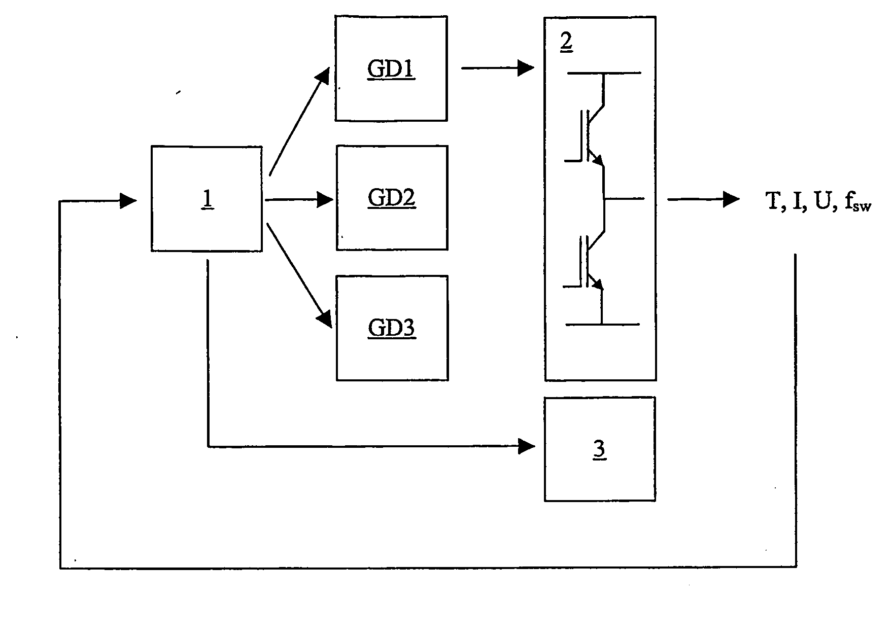
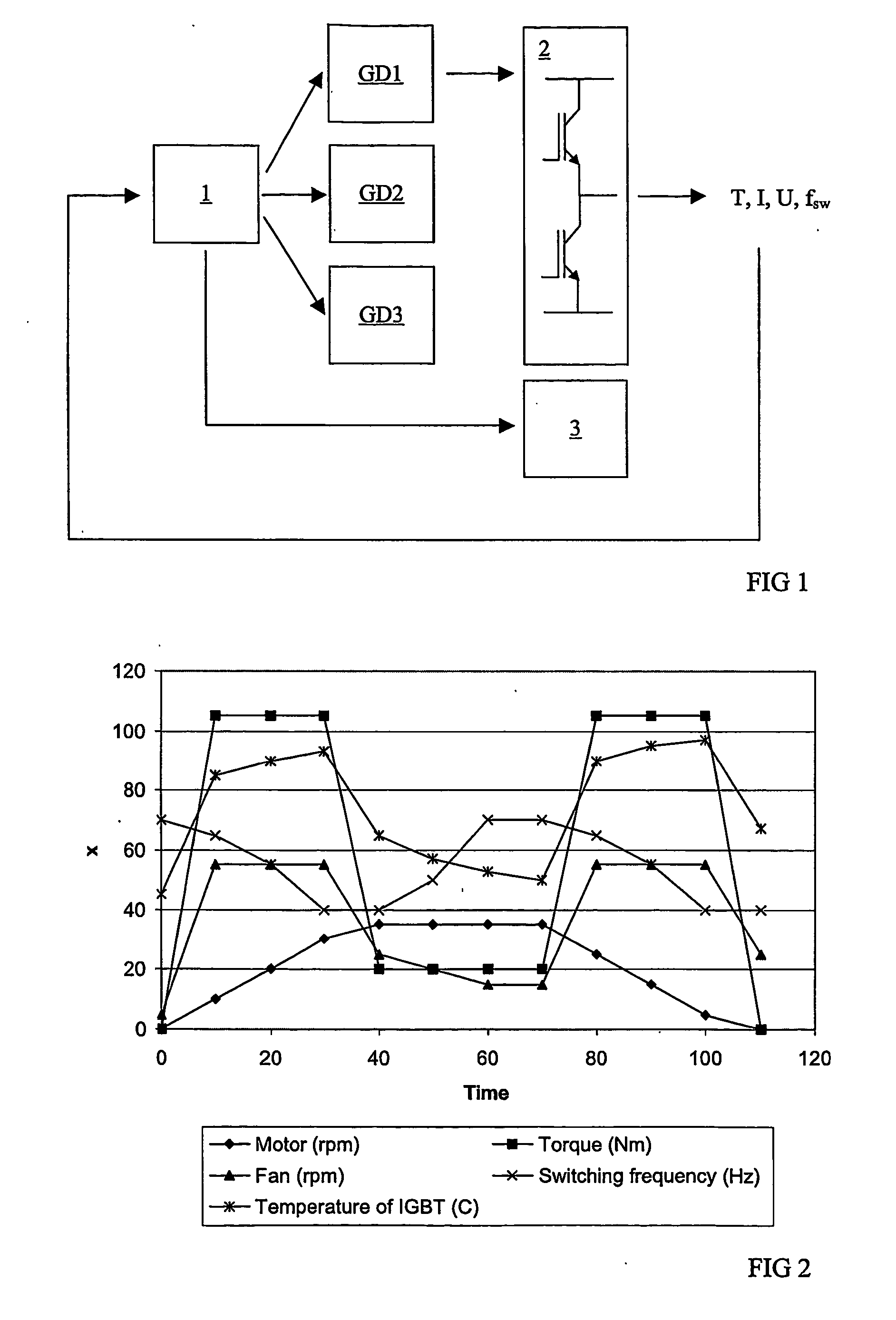
[0017]FIG. 1 shows on a general level a block diagram of the arrangement of the invention implementing the method of the invention. The arrangement is shown in association with an inverter, and no specific target of application is shown for the inverter. Thus, it is clear that the method and arrangement can be utilized in any application using an inverter.

[0018]FIG. 1 shows how a processor element 1 controls gate drivers GD1, GD2, GD3 in accordance with a control algorithm in the processor. The gate drivers are correspondingly connected to control power semiconductors 2, of which FIG. 1 only shows two, i.e. a switch pair that typically forms one phase. In a normal three-phase system, there are three switch pairs of this type.

[0019] According to the method of the invention, the temperature T or an electric quantity affecting the temperature of one or more power semiconductor components 2 is determined. The determination of the temperature can at its simplest be done by measuring th...


PUM


Abstract

A method and arrangement in connection with an inverter that comprises several power semiconductor components and a control apparatus arranged to control them, the control apparatus being arranged to control the power semiconductor components in response to a control quantity to generate an output voltage. The method comprises the steps of determining the change of the temperature or a quantity affecting the temperature of one or more power semiconductor components, and controlling with the control apparatus the power semiconductor components in response to both the control quantity to generate an output voltage and the change rate of the temperature or quantity affecting the temperature of the power semiconductor components to reduce the temperature change and the change rate.

Description

BACKGROUND OF THE INVENTION [0001] The present invention relates to a method and arrangement in an inverter for the purpose of reducing the effects related to the temperature variation of semiconductor components. [0002] An inverter is an electric device in which it is possible to generate a voltage with variable frequencies. Inverters are typically used in motors to control them at an altering frequency or when transferring electric power back to the network, in which case the inverter generates a voltage whose frequency corresponds to that of the network. Such an inverter supplying the network is generally called a network inverter. [0003] Today, IGB transistors (Insulated Gate Bipolar Transistor, IGBT), which are fast, gate-controlled components, are typically used as power semiconductors of inventers, i.e. the switch components generating the output voltage. The current-carrying capacity of the largest IGBT components is several hundreds of amperes and their maximum voltage is t...

Claims


Application Information

Patent Timeline
IPC IPC(8): G11C7/04G01K7/01G01K15/00H01L23/34H02M1/00H02M1/32
CPCG01K7/01G01K15/00H01L23/34H01L25/16H01L2924/0002H02M1/32H01L2924/00
Inventor RONKAINEN, TEEMUHYVARINEN, VEIKKOTIITINEN, PEKKA
Owner ABB (SCHWEIZ) AG
Why Eureka
Try Eureka