Method of forming a layer and method of manufacturing a capacitor using the same
- Summary
- Abstract
- Description
- Claims
- Application Information
AI Technical Summary
Benefits of technology
Problems solved by technology
Method used
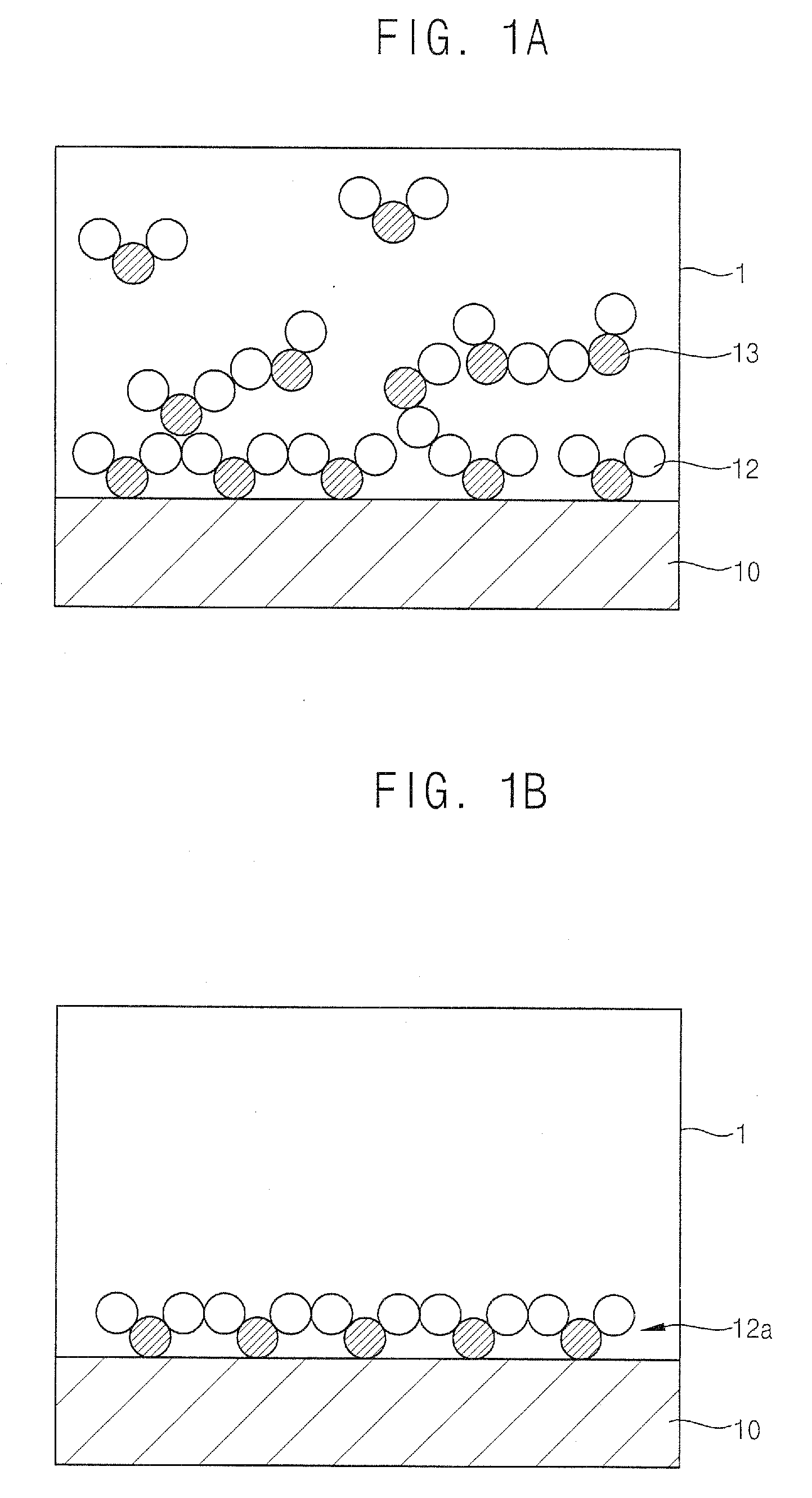
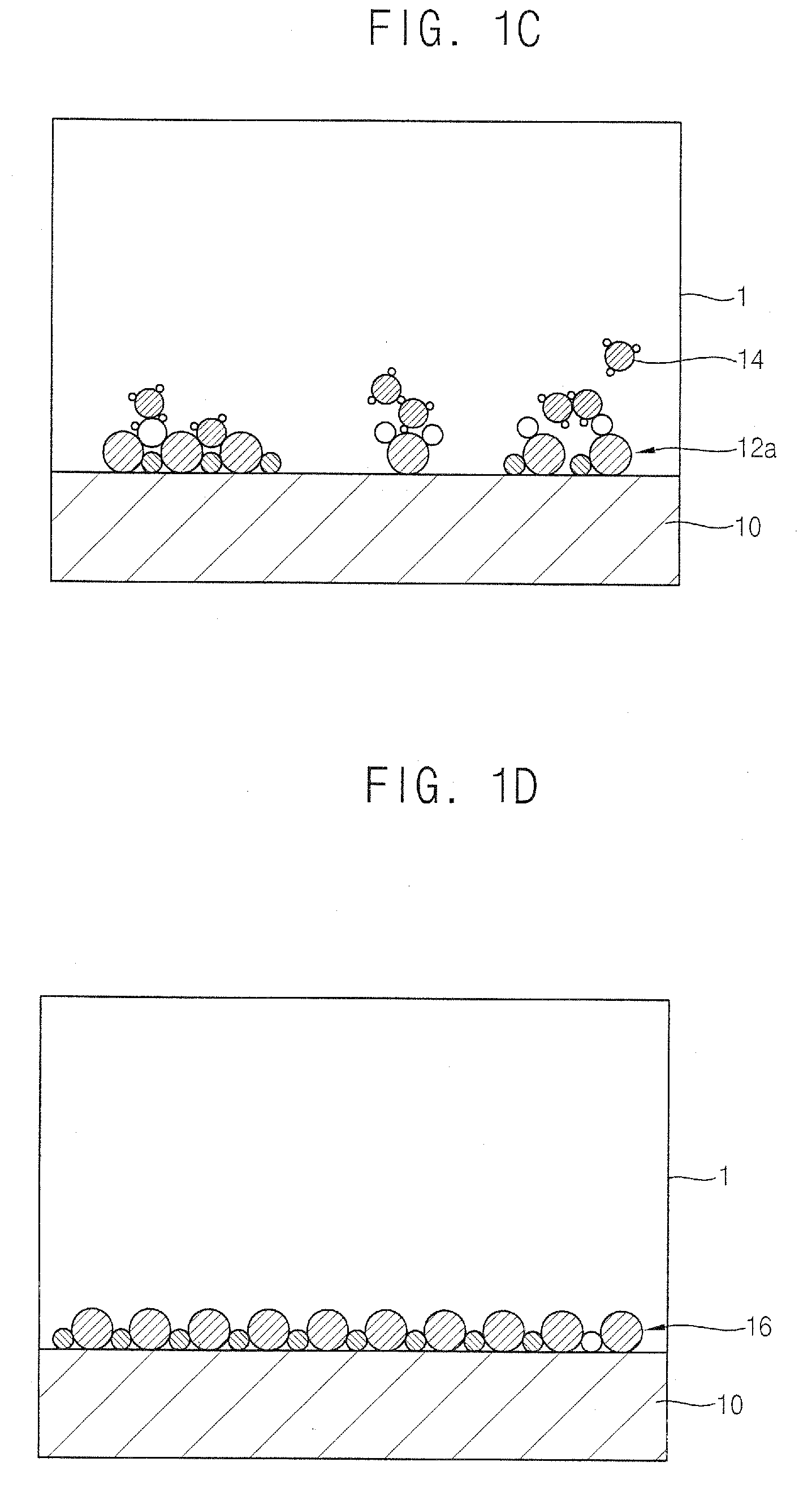
Image

Examples
examples
[0113] Evaluation of an EOT Variation According to a Thermal Treatment
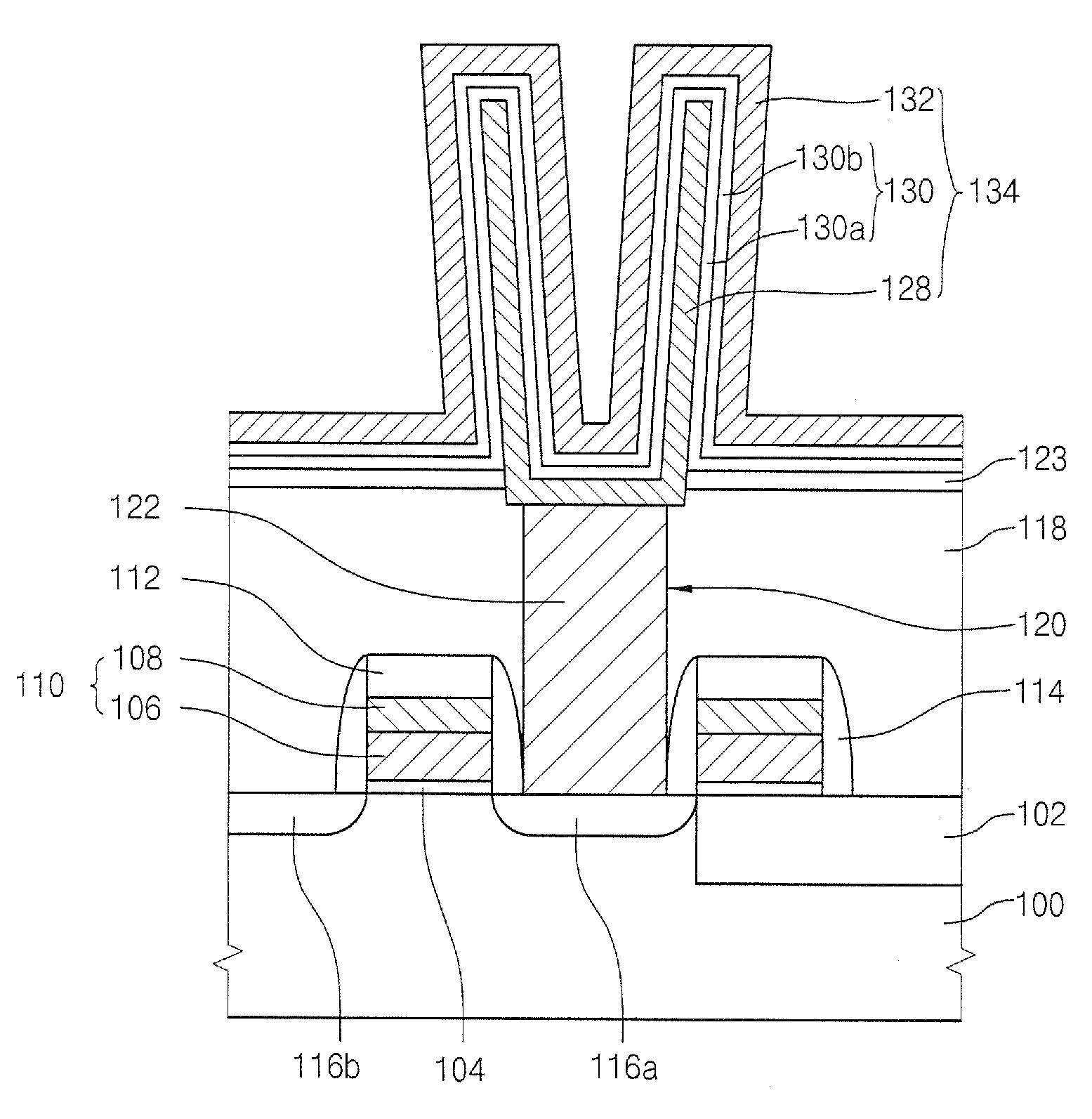
[0114] Specimen 1 was prepared by sequentially forming a lower electrode, a dielectric layer having a first zirconium oxide film, an aluminum oxide film and a second zirconium oxide film, and an upper electrode on a silicon wafer. The lower and the upper electrodes were formed using titanium nitride. The dielectric layer was formed by an ALD process. The first zirconium oxide film had a thickness of about 30 Å, the aluminum oxide film had a thickness of about 5 Å, and the second zirconium oxide film had a thickness of about 60 Å.
[0115] Specimen 2 was prepared by sequentially forming a lower electrode having titanium nitride, a dielectric layer having a first zirconium oxide film, an aluminum oxide film and a second zirconium oxide film, and an upper electrode having titanium nitride on a silicon wafer. The dielectric layer was formed by an ALD process. The first zirconium oxide film had a thickness of about 45 Å...
PUM
| Property | Measurement | Unit |
|---|---|---|
| Temperature | aaaaa | aaaaa |
| Temperature | aaaaa | aaaaa |
| Thickness | aaaaa | aaaaa |
Abstract
Description
Claims
Application Information
 - R&D
- Intellectual Property
- Life Sciences
- Materials
- Tech Scout
- Unparalleled Data Quality
- Higher Quality Content
- 60% Fewer Hallucinations
Browse by: Latest US Patents, China's latest patents, Technical Efficacy Thesaurus, Application Domain, Technology Topic, Popular Technical Reports.
© 2025 PatSnap. All rights reserved.Legal|Privacy policy|Modern Slavery Act Transparency Statement|Sitemap|About US| Contact US: help@patsnap.com