Method for annealing silicon thin films and polycrystalline silicon thin films prepared therefrom

a polycrystalline silicon and thin film technology, applied in the field of annealing silicon thin films and polycrystalline silicon thin films, can solve the problems that the low temperature crystallization method using elc or sls is only limited in the flat plate industry, and achieves the effects of short time, short heat deflection of the substrate, and simple and economically favorable crystallization process

Inactive Publication Date: 2007-05-03
ENSIL TECH CO LTD
View PDF4 Cites 18 Cited by
  • Summary
  • Abstract
  • Description
  • Claims
  • Application Information

AI Technical Summary

Benefits of technology

[0028] First, the process for accomplishing crystallization is very simple and economically favorable. ELC, one of the latest techniques, scans line beams to be overlapped and SLS adopts a method of precisely moving a very short distance after irradiating laser through a patterned mask, so they take so long time to crystallize an entire substrate. However, the method of the present invention is capable of conducting crystallization and eliminating defects on an a-Si thin film, an a-Si / Poly-Si thin film or a Poly-Si thin film over the entire substrate within a very short time without any heat deflection of the substrate. Furthermore, ELC or the like is very complex unlike the method of the present invention, since it needs an additional dehydration annealing process for removing hydrogen from an a-Si thin film as a preprocess to irradiation of a laser. Meanwhile, though the conventional techniques such as MIC and MILC should deposit a catalyst metal thin film in order to promote crystallization, the method of the present invention does not require a catalyst metal deposition process for crystallization, so the method of the present invention is very simple and does not cause metallic contamination, in comparison to the conventional art.
[0029] Second, the present invention may be accomplished using inexpensive equipments and an existing technique already established. While ELC or the like, which gives excellent crystallization effects, requires very expensive equipments like a laser device, a preheating furnace or RTA necessary for the present invention is relatively cheap. In addition, the techniques for the method of the present invention are already well established in the semiconductor and flat display industries, so it is possible to use the conventional techniques as they are or through a little reorganization. In order to produce a uniform Poly-Si thin film by the method of the present invention, there may be needed stable power supply and time regulator for keeping a resistance value of the silicon thin film constant and applying an electric field. However, though the constant resistance of the silicon thin film may be seriously affected by the uniformity of a film thickness and a substrate temperature, the technique for forming an a-Si thin film with a uniform thickness is already perfected through PECVD, LPCVD and so on, and the thermal treatment may also be easily obtained since the temperature uniformity is already well established in the industry.
[0030] Third, the present invention is suitable for mass-production of Poly-Si thin films of good quality from a large-size substrate. According to the present invention, since the overall substrate is crystallized at once very rapidly, it is very advantageous for treatment of a large-sized substrate, and the Poly-Si thin films obtained may give crystallized materials of good quality without surface protrusions.
[0031] Fourth, the present invention may be used for a low temperature dopant activating process. The selective Joule heating by field application of the present invention may be effectively applied for thermal treatment of a dopant, to which ion is injected, near a source / drain electrode in TFT structure at a low temperature, as well as for crystallization.

Problems solved by technology

Thus, as a matter of fact, the low temperature crystallization method using ELC or SLS is only limited applied in the flat plate industry.

Method used


Image

  • Method for annealing silicon thin films and polycrystalline silicon thin films prepared therefrom
  • Method for annealing silicon thin films and polycrystalline silicon thin films prepared therefrom
  • Method for annealing silicon thin films and polycrystalline silicon thin films prepared therefrom

Examples


example 1

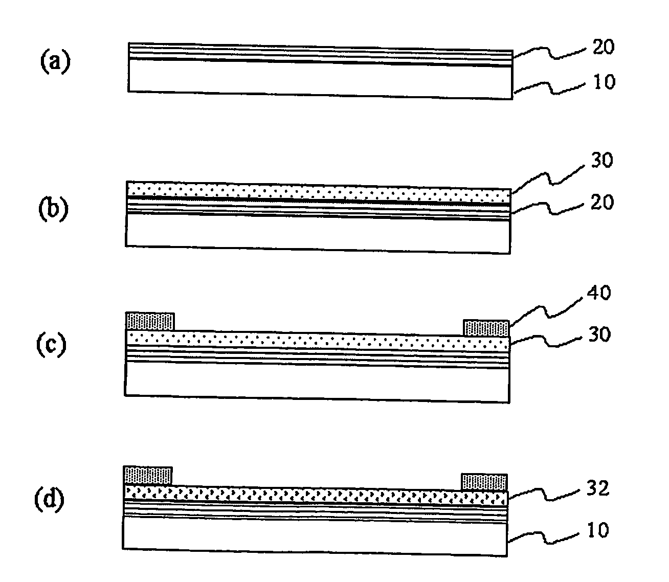
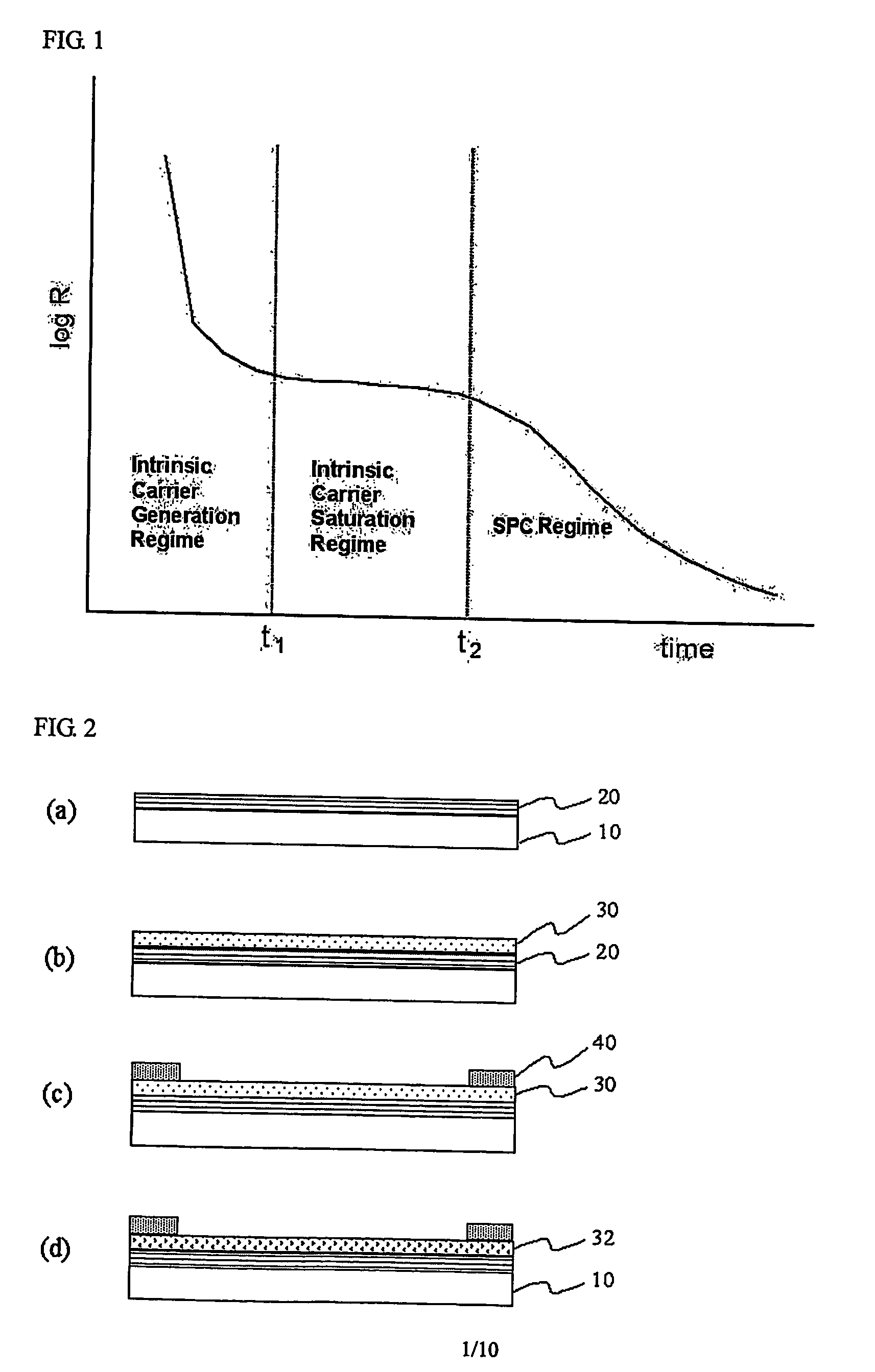
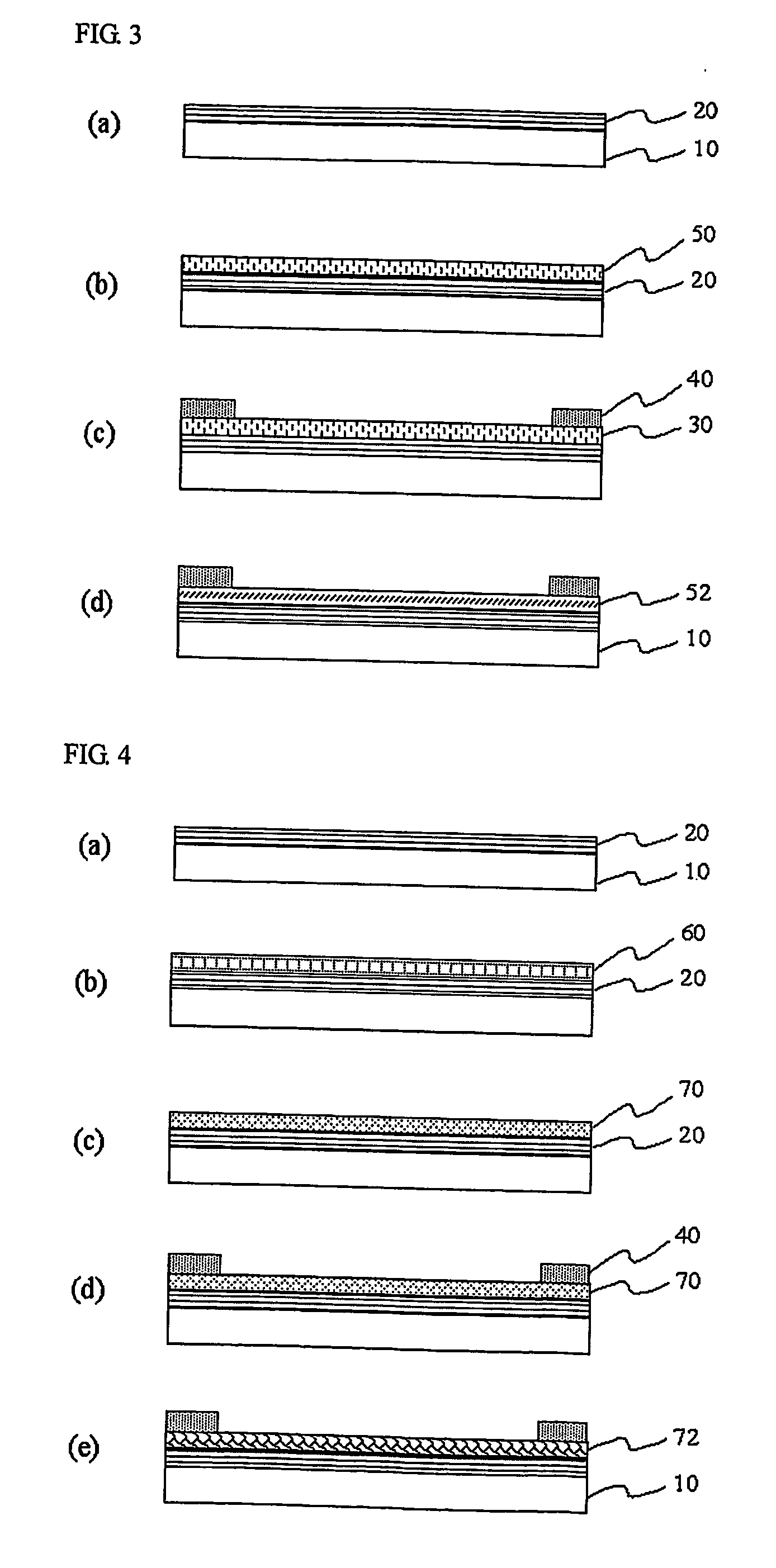
[0095] SiO2 insulation layer with a thickness of 3000 Å was formed on a glass substrate of 2 cm×2 cm×0.7 mm (length×width×thickness) by means of PECVD. An a-Si thin film with a thickness of 500 Å was formed again upon the insulation layer by means of PECVD, thereby preparing a test piece. The a-Si thin film formed as mentioned above was preheated in a tube furnace at about 650° C. for about 30 minutes under nitrogen atmosphere. After the preheating step and before applying an electric field, the a-Si thin film already experienced solid crystallization and contained partially polycrystalline phase, and a surface resistance of the thin film was about 35 kΩ. After the resistance of the silicon thin film was sufficiently lowered by means of such preheating, a DC electric field of 1,500 V / cm was applied so that a current of 250 mA flowed for 0.07 seconds, and then an electric field was applied again at a time interval of about 2.5 second to induce selective Joule heating in the silicon t...

example 2

[0101] SiO2 insulation layer with a thickness of 3000 Å was formed on a glass substrate of 2 cm×1 cm×0.7 mm (length×width×thickness) by means of PECVD. An a-Si thin film with a thickness of 500 Å was formed again upon the insulation layer by means of PECVD, thereby preparing a test piece. The a-Si thin film formed as mentioned above was crystallized into a Poly-Si thin film by means of a laser crystallization method, and then the Poly-Si thin film is doped by ion shower with the use of PH3 / H2 mixture gas. For the low temperature dopant activation of the test piece to which ion is injected, after preheating at 250° C. for about 20 minutes, a DC electric field of 1,000 V / cm is applied. Except that, the experiment was conducted in the same way as the Example 1. The glass substrate of the test piece treated as mentioned above kept its original flatness without deflection, and a surface resistance of the Poly-Si thin film to which an electric field was applied and then ion was injected w...


PUM

PropertyMeasurementUnit
electric fieldaaaaaaaaaa
sizeaaaaaaaaaa
temperatureaaaaaaaaaa

Abstract

Disclosed is a method for annealing a silicon thin film in a substrate in which an insulation layer and the silicon thin film are subsequently formed. The method includes heating or preheating the silicon thin film within a temperature range at which the substrate is not transformed during the process so as to generate an intrinsic carrier therein, thereby lowering a resistance to a value at which Joule heating is possible; and applying an electric field to the preheated silicon thin film so as to induce Joule heating by means of movement of the carrier, thereby conducting crystallization, eliminating crystal defects, and ensuring crystal growth. When using the method, Joule heating is selectively induced to a-Si thin film, a-Si/Poly-Si thin film or a Poly-Si thin film according to the preheating condition, thereby making a Poly-Si thin film of good quality within a very short time without damaging the substrate.

Description

BACKGROUND OF THE INVENTION [0001] 1. Field of the Invention [0002] The present invention relates to a method for annealing silicon thin films and polycrystalline silicon thin films prepared using the method. More particularly, the present invention relates to a method for annealing silicon thin films, which, in a substrate on which an insulation layer and a silicon film are subsequently formed, preheats the silicon film in a temperature range where the substrate is not transformed during the process in order to generate an intrinsic carrier therein so that a resistance is lowered to a value enabling Joule heating, applies an electric field to the preheated silicon film in order to induce Joule heating by means of movement of the carrier, resulting in crystallization, removal of crystal lattice defects, and crystal growth, and also relates to polycrystalline silicon thin films of good quality, prepared using the method. [0003] 2. Description of the Related Art [0004] Generally, amor...

Claims


Application Information

Patent Timeline
Patent Type & Authority Applications(United States)
IPC IPC(8): H01L21/84H01L21/00H01L21/324H01L21/20H01L21/326H01L21/336H01L21/77H01L29/786
CPCH01L21/2022H01L21/326H01L27/1285H01L29/78618H01L29/6675H01L21/02667H01L21/02488H01L21/02422H01L21/02532H01L21/0242H01L21/02595H01L27/1214
Inventor RO, JAE-SANGHONG, WON-EUI
Owner ENSIL TECH CO LTD
Why Eureka
Try Eureka