LED having a reflector layer of improved contact ohmicity and method of fabrication

Active Publication Date: 2007-05-10
SANKEN ELECTRIC CO LTD
View PDF2 Cites 25 Cited by
  • Summary
  • Abstract
  • Description
  • Claims
  • Application Information

AI Technical Summary

Benefits of technology

[0014] Experiment has proved that, admixed with any of the above listed additives in the specified range of proportions, silver gains immunity from oxidation and sulfurization without suffering any significant drop in reflectivity.

Problems solved by technology

An obvious drawback to this approach was the inevitable light absorption by the substrate, both before and after reflection by the reflector.
Lying in the way of bidirectional light travel, the substrate considerably lessened the efficiency of the LED.
Another difficulty was the high electrical resistance between the light-generating semiconductor region and the substrate.
This second mentioned difficulty brought about an additional inconvenience in those LEDs in which the substrate provides part of the current path, with a cathode, say, attached to the substrate.
The forward voltage between the anode and cathode became inconveniently high in such LEDs.
The last cited prior art LED proved to possess its own weaknesses, however.
Although capable of low-resistance contact with the light-generating semiconductor region, the open-worked layer of gold-germanium-gallium alloy poorly lacks in reflectivity.
The solid metal-made reflector layer on the other hand is

Method used


Image

  • LED having a reflector layer of improved contact ohmicity and method of fabrication
  • LED having a reflector layer of improved contact ohmicity and method of fabrication
  • LED having a reflector layer of improved contact ohmicity and method of fabrication

Examples


embodiment

of FIG. 8

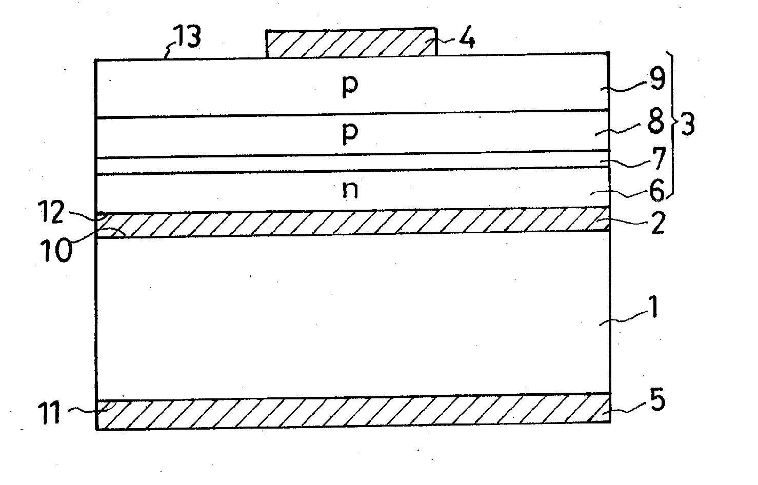
[0065]FIG. 8 shows another preferred form of LED embodying the principles of the present invention. This LED differs from that of FIG. 1 in:

[0066] 1. A difference in size between baseplate 1 and light-generating semiconductor region 3.

[0067] 2. The position and shape of the second electrode or cathode 5.

[0068] 3. The introduction of a current blocking layer or current baffle 21.

[0069] 4. The shape of a reflector layer 2a.

[0070] As seen from above the LED, the baseplate 1 is larger than the light-generating semiconductor region 3. With the light-generating semiconductor region 3 placed centrally on its upper major surface 10, the baseplate 1 has an annular ledge protruding outwardly of the semiconductor region 3. The cathode 5 is formed on this annular ledge of the baseplate 1 in electrical contact therewith and is correspondingly modified in shape.

[0071] The current baffle 21 is interposed between the upper major surface 10 of the baseplate 1 and the lower major surfa...


PUM


Abstract

An LED has a light-generating semiconductor region formed on a baseplate via an electroconductive reflector layer. The light-generating semiconductor region has an active layer sandwiched between a pair of claddings of opposite conductivity types for generating light. For good ohmic contact with the light-generating semiconductor region without any substantive diminution of reflectivity compared to that of unalloyed silver, the reflector layer is made from a silver-base alloy containing a major proportion of silver and at least either one of copper, gold, palladium, neodymium, silicon, iridium, nickel, tungsten, zinc, gallium, titanium, magnesium, yttrium, indium, and tin.

Description

CROSS REFERENCE TO RELATED APPLICATIONS [0001] This is a continuation of Application PCT / JP2005 / 012210, filed Jul. 1, 2005, which claims priority to Japanese Patent Application No. 2004-200849 filed Jul. 7, 2004.BACKGROUND OF THE INVENTION [0002] This invention relates to light-emitting semiconductor devices, or light-emitting diodes (LEDs) according to more common parlance, and more particularly to such devices of the class suitable for use in displays and lamps, among other applications. The invention also concerns a method of making such light-emitting semiconductor devices. [0003] The LED has been known which has a light-generating semiconductor region comprised of an active layer sandwiched between an n-type cladding or lower confining layer, which overlies the substrate, and a p-type cladding or upper confining layer. Part of the light generated in the active layer mostly directly traverses the upper confining layer and issues from one of the opposite major surfaces of the sem...

Claims


Application Information

Patent Timeline
IPC IPC(8): H01L33/00H01L33/10H01L33/32H01L33/50
CPCH01L33/0079H01L33/405H01L33/0093
Inventor AOYAGI, HIDEKAZUOTSUKA, KOJI
Owner SANKEN ELECTRIC CO LTD
Why Eureka
Try Eureka