Optical waveguide devices

a waveguide and optical waveguide technology, applied in the direction of optical waveguide light guides, optical light guides, instruments, etc., can solve the problems of increased insertion loss and cross talk at the crossing part, difficult to lower the curvature radius of increased optical radiation loss in the curved part of the optical waveguide. achieve the effect of constant thickness

Active Publication Date: 2007-05-10
NGK INSULATORS LTD
View PDF6 Cites 18 Cited by
  • Summary
  • Abstract
  • Description
  • Claims
  • Application Information

AI Technical Summary

Benefits of technology

[0035]FIG. 1 is a plan view showing an optical modulator 2, and FIG. 2 is a cross sectional view showing the optical modulator 2 of FIG. 1.
[0036] The optical modulator 2 has an optical waveguide substrate 3 and a supporting body 31. Both of the substrate 3 and supporting body 31 are flat-plate shaped. The substrate 3 has a thickness of 30 μm or smaller (in a region where the optical waveguide is formed). Predetermined electrodes 4A, 4B and 4C are formed on a main face of the substrate 3.
[0037] Although it is applied a so-called coplanar waveguide type electrode (CPW electrode) configuration according to the present example, the configuration of electrodes is not particularly limited. According to coplanar electrode configuration, a line of signal electrode is provided between a pair of ground electrodes. The present invention is, however, applicable to so-called ACPS type traveling wave optical modulator, for example. In this case, one line of ground electrode and one line of signal electrode are provided. It may be further applicable a traveling wave type optical modulator of, so-called, independent modulation type.
[0038] According to the present example, an optical waveguide 5 forms so-called Mach-Zehnder type waveguide in a plan view. That is, light is incident into an input part 5a of the optical waveguides 5, divided into two branched parts 5b and then incident into modulating parts 5A, 5B, respectively, through covered parts 5c. The light is then incident into branched parts 5e,

Problems solved by technology

As the optical waveguide is curved, however, an optical radiation loss is increased in the curved part of the optical waveguide.
It has thus been difficult to lower the radius of curvature of the curved part of the optical waveguide.
I

Method used


Image

  • Optical waveguide devices
  • Optical waveguide devices
  • Optical waveguide devices

Examples


example 1

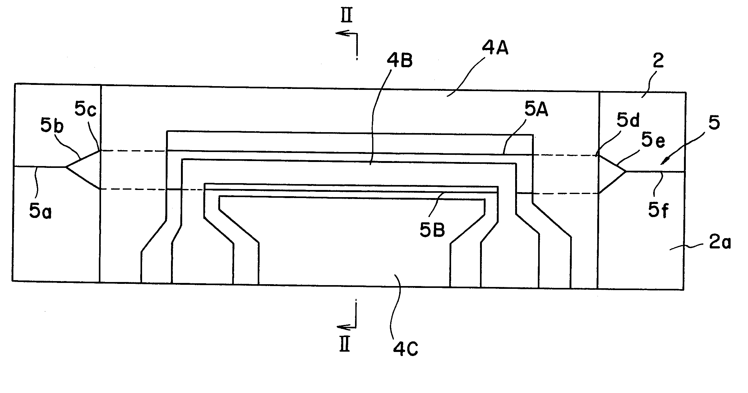
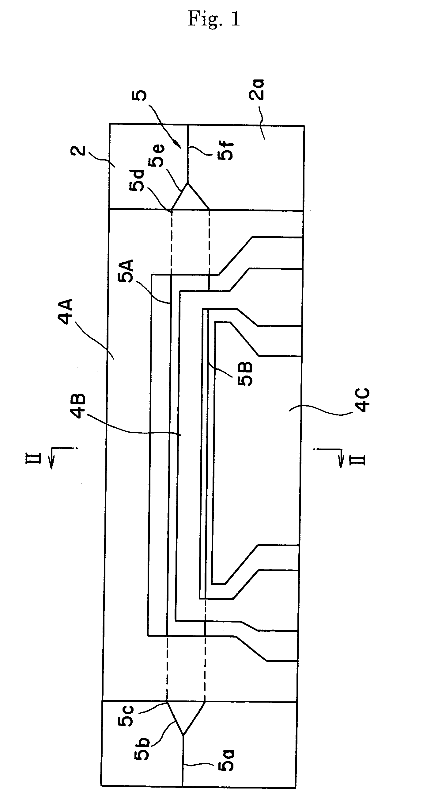
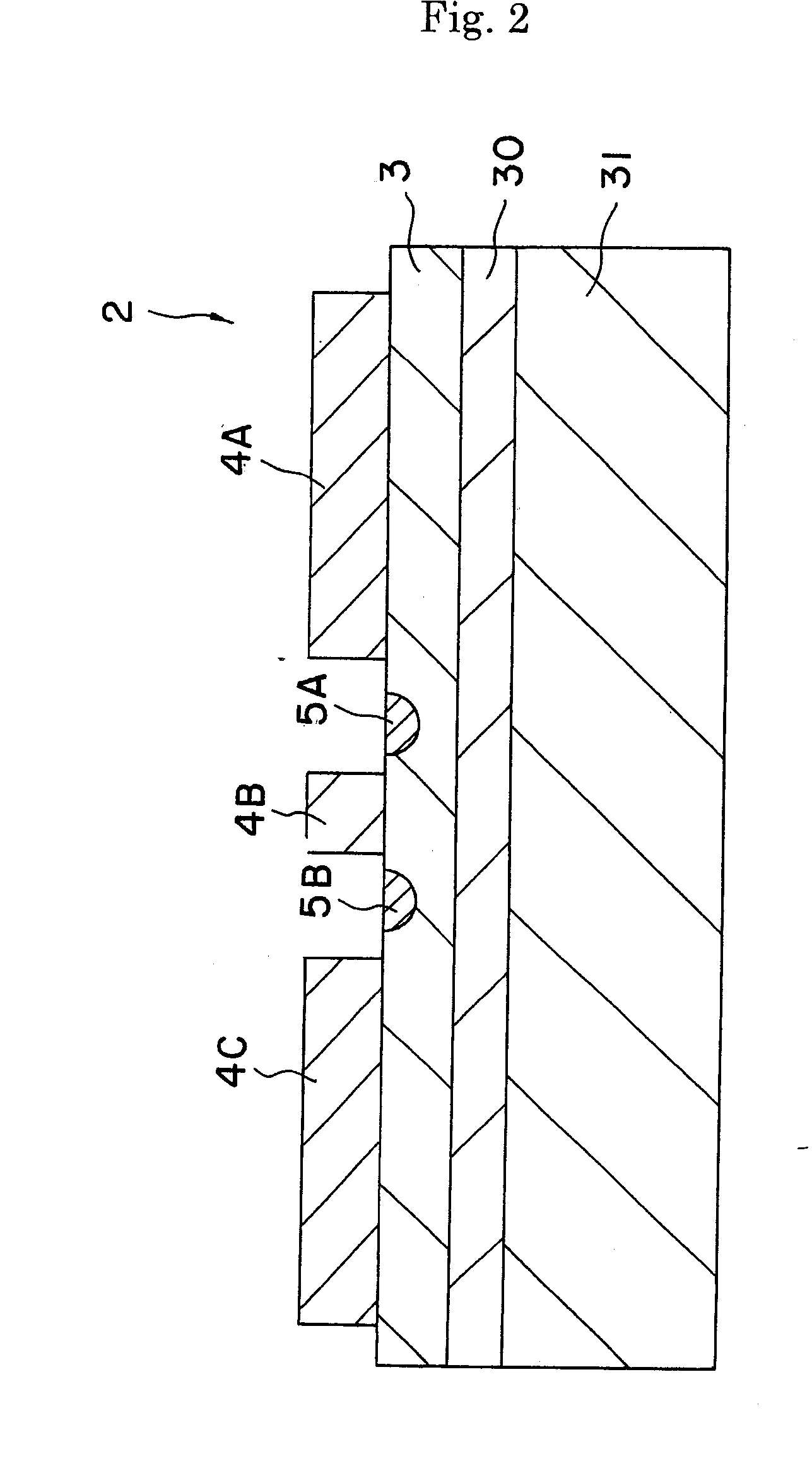
[0062] The optical modulator 1 of FIG. 1 was used. Specifically, an X-cut 3 inch wafer (made of LiNbO3 single crystal) was used as a substrate. An optical waveguide 5 of Mach-Zehnder type was formed in the surface area of the wafer by titanium diffusion and photolithography. The size of the optical waveguide 5 may be set at, for example, 10 μm at 1 / e2. The CPW electrode pattern was formed by electroplating. The gap between the signal and ground electrodes were made 40 μm, the electrode thickness was made 28 μm and the electrode length was 40 mm. A dummy body for polishing was adhered onto a surface plate for polishing for performing thinning and polishing. The substrate for modulator was adhered thereon with a thermoplastic resin while the electrode face was orientated downwardly. The substrate 4 was thinned to a thickness of 10 μm by means of horizontal polishing and polishing (CMP). The substrate was then adhered onto a plate-shaped supporting body 31, and the substrate was subjec...

experiment 2

[0065] An optical modulator was fabricated according to the same procedure as the Experiment 1. The radiation loss per an angle of curvature of 5° was measured for each optical modulator. The substrate thickness was 6 μm, Tti (thickness of titanium film before the titanium diffusion) was 0.70 μm and Wti (width of titanium film before the titanium diffusion) was 5 μm, 7 μm, 9 μm or 11 μm. The results were shown in FIG. 8.

[0066] As can be seen from FIG. 8, the radiation loss per an angle of curvature of 5° can be considerably reduced, by elevating Wti (width of titanium film before the titanium diffusion) to, especially, 7 μm or larger.

experiment 3

[0067] An optical modulator having the shape of FIGS. 1, 2, 5 or 9 was produced, according to the same procedure as the Experiment 1. The following examples were performed: (1) the groove was not provided, (2) the grooves 20 and 35 were provided and the groove 21 was not provided and (3) both of the grooves 20A and 21 were provided. Each of the widths “W1” and “W2” of the grooves 20, 20A, 21 and 35 was made 5 μm, and the distances “d1” and “d2” between the grooves 20, 21 and the beam center of the optical waveguide were made 4 μm, respectively. The depth “Dg” of each of the grooves 20, 20A, 21 and 35 was made 2 μm. The thickness of the optical waveguide substrate 3 and the radius “R” of curvature of each of the curved parts 5c to 5f were changed as shown in table 2. The radiation loss per an angle of curvature of 180° was estimated by means of beam propagation method. The results were shown in table 2.

TABLE 2Thickness ofThickness ofLN substrate:LN substrate:8 μm8 μmRadius ofRadius...


PUM


Abstract

It is provided an optical waveguide device in which the radius of curvature of a curved part of an optical waveguide can be lowered and the radiation loss of light in the curved part can be reduced. An optical waveguide device 2 has a ferroelectric optical waveguide substrate and an optical waveguide 5 formed in or on the substrate and modulating electrodes 4A, 4B and 4C. The thickness of the optical waveguide substrate is 30 μm or smaller at least in a region where the optical waveguide is formed. The optical waveguide has curved part having a radius of curvature of 30 mm or smaller.

Description

[0001] This application claims the benefits of Japanese Patent Application P2005-325928 filed on Nov. 10, 2005, the entirety of which is incorporated by reference. BACKGROUND OF THE INVENTION [0002] 1. Field of the Invention [0003] The present invention relates to an optical waveguide device. [0004] 2. Related Art Statement [0005] It is proposed a structure of lowering the thickness of an optical waveguide substrate to attain the velocity matching of microwave and light wave, so as to widen the modulation bandwidth of an optical modulator. [0006] In such kind of a structure utilizing a thinner optical waveguide substrate, it is required to lower the thickness of the substrate around an optical waveguide to a value of, for example 10 μm, for satisfying the velocity matching condition. Such thin optical waveguide may result in the flattening of optical mode field pattern and transmission loss of light due to surface roughness and damage caused by the processing for producing the thin ...

Claims


Application Information

Patent Timeline
IPC IPC(8): G02F1/295
CPCG02B6/125G02B2006/12097G02B2006/12104G02B2006/12119G02B2006/12142G02B2006/12159G02F1/0508G02F1/2255G02F1/3137
Inventor MITOMI, OSAMUAOKI, KENJIKONDO, JUNGOIWATA, YUICHIEJIRI, TETSUYA
Owner NGK INSULATORS LTD
Why Eureka
Try Eureka