Method of sealing semiconductor element mounted on gold-plated printed circuit board

Active Publication Date: 2007-05-10
SHIN ETSU CHEM IND CO LTD
View PDF4 Cites 5 Cited by
  • Summary
  • Abstract
  • Description
  • Claims
  • Application Information

AI Technical Summary

Benefits of technology

[0017] By employing a sealing method of the present invention, the resulting sealed product (laminate) exhibits particularly superior adhesion between the gold-plated printed circuit board and the silicone resin, while the silicone resin exhibits favorable external appearance and hardness, and no noticeable tackiness. In addition, the silicone resin also exhibits favorable durability under heat cycling, condition

Problems solved by technology

Epoxy resins have conventionally been used as the sealing materials, but improvements in the performance levels of elements, and the resulting increases in optical energy and heat generated by the elements, have lead to discoloration and degradation of the epoxy resins becoming a significant issue (see non-patent reference 1).
Silicone resins are possible alternative r

Method used


Image

  • Method of sealing semiconductor element mounted on gold-plated printed circuit board
  • Method of sealing semiconductor element mounted on gold-plated printed circuit board
  • Method of sealing semiconductor element mounted on gold-plated printed circuit board

Examples


Example

Example 1

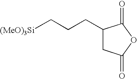
[0090] A gold-plated printed circuit board with a semiconductor element mounted thereon was immersed for 5 seconds in a solution comprising 0.5 parts by mass of an acid anhydride group-containing alkoxysilane represented by a structural formula (7) shown below:

and 99.5 parts by mass of ethanol, and the circuit board was then dried in an oven at 100° C. for 10 minutes. This circuit board was then subjected to potting with a composition A comprising 60 parts by mass of a compound represented by a structural formula (8) shown below:

(wherein, u=0.5), 40 parts by mass of a compound represented by a structural formula (9) shown below:

(wherein, v=5), a sufficient quantity of an isopropanol solution of chloroplatinic acid to provide a mass-referenced quantity of platinum metal atoms of 40 ppm relative to the combined mass of the compounds represented by the above structural formulas (8) and (9), and a sufficient quantity of bis(1-octyloxy-2,2,6,6-tetramethyl-4-piperidyl)s...

Example

Example 2

[0091] A composition B was prepared by adding 2 parts by mass of the acid anhydride group-containing alkoxysilane represented by the above structural formula (7) to 100 parts by mass of the composition A disclosed in the example 1. This composition B was used for conducting potting of an untreated gold-plated printed circuit board, thereby forming a coating film with a thickness of approximately 0.1 mm, and this film was then cured by heating at 100° C. for 1 hour, and then at 150° C. for 5 hours. This completed the preparation of a sealed structure.

Example

Comparative Example 1

[0092] With the exception of replacing the acid anhydride group-containing alkoxysilane in the example 1 with 2-(3,4-epoxycyclohexyl)ethyltrimethoxysilane, a sealed structure was prepared in the same manner as the example 1.


PUM

PropertyMeasurementUnit
Timeaaaaaaaaaa

Abstract

Methods of sealing a semiconductor element are provided. The methods includes the steps of coating a semiconductor element mounted on a gold-plated printed circuit board with a curable silicone resin, and then curing the curable silicone resin. In a method, the gold-plated printed circuit board is subjected to preliminary treatment with a treatment agent including an acid anhydride group-containing alkoxysilane and/or a partial hydrolysis-condensation product thereof In another method, the curable silicone resin includes the treatment agent. The methods yield favorable adhesion upon sealing.

Description

BACKGROUND OF THE INVENTION [0001] 1. Field of the Invention [0002] The present invention relates to a method of sealing a semiconductor element that is mounted on a gold-plated printed circuit board. [0003] 2. Description of the Prior Art [0004] Examples of conventional optical semiconductors include light-receiving elements such as the photodiodes of various optical sensors and phototransistors, as well as light-emitting diodes (LED). One known method of molding such optical semiconductors involves, for example, mounting the semiconductor element on a gold-plated printed circuit board, and following wire-bonding, sealing the semiconductor element using a molding technique such as potting or transfer molding. [0005] Epoxy resins have conventionally been used as the sealing materials, but improvements in the performance levels of elements, and the resulting increases in optical energy and heat generated by the elements, have lead to discoloration and degradation of the epoxy resins ...

Claims


Application Information

Patent Timeline
IPC IPC(8): B05D3/10C08L83/04B32B27/00H01L21/56H01L23/29H01L23/31
CPCC08L83/06H01L23/296H01L23/3142H01L33/56H01L2924/0002H01L2924/00
Inventor TABEI, EIICHIYANAGISAWA, HIDEYOSHI
Owner SHIN ETSU CHEM IND CO LTD
Why Eureka
Try Eureka